Siemens MC45, Manual
The Siemens MC45 is a versatile mobile phone designed for reliable communication on the go. With its user-friendly interface, accessing its features is a breeze. Explore its full capabilities by downloading the free user manual from our website, empowering you to make the most out of this remarkable device.
Share
Download


Reviews:
No comments
Related manuals for MC45
Optimus 5100
Brand: Radio Shack Pages: 2
projectorsleeve
Brand: 3M Pages: 14
Blue2
Brand: AbleNet Pages: 9
Air
Brand: Easymount Pages: 2
AC171
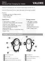
Brand: Valore Pages: 5
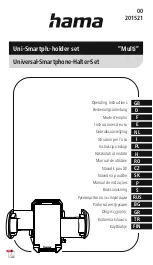
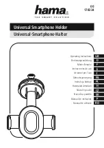
Multi
Brand: Hama Pages: 40
MINIKIT CHIC
Brand: Parrot Pages: 11
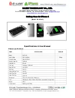
DGIPOD-4655 - DATASHEET FOR IPHONE
Brand: I.SOUND Pages: 1
GV-WM4
Brand: Groov-e Pages: 2
Fun 70 BT
Brand: Hama Pages: 14
HookUpz Smartphone Telescope Adapter
Brand: Carson Pages: 16

POWERSHELL
Brand: Logitech Pages: 152
FANCY STAND
Brand: Hama Pages: 112

Pocket Dual Catchmon
Brand: Megacom Pages: 2
EL-IP4-01
Brand: E-LINK Pages: 4
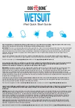
Wetsuit
Brand: Dog & Bone Pages: 8
178334
Brand: Hama Pages: 27
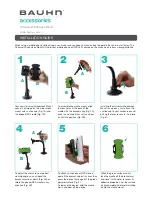
AA-05
Brand: Bauhn Pages: 2


