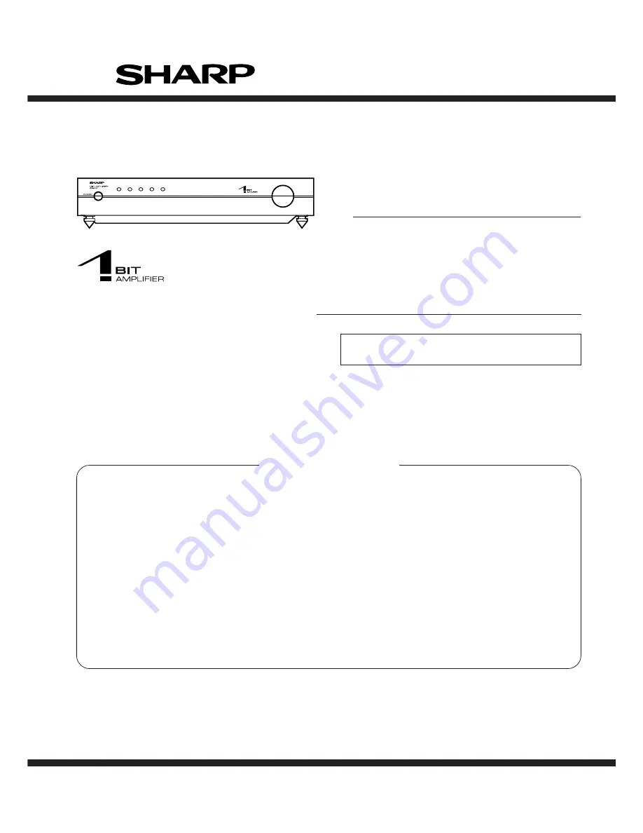
background image

SM-SX1/SX1W

– 1 –

SM-SX1

• In the interests of user-safety the set should be restored to its

original condition and only parts identical to those specified be
used.

SERVICE MANUAL

SHARP  CORPORATION

No. S7063SMSX1///

This document has been published to be used
for after sales service only.
The contents are subject to change without notice.

 CONTENTS

Page

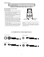
IMPORTANT SERVICE NOTES (SM-SX1 FOR U.S.A. ONLY) ......................................................................................... 2
AC POWER SUPPLY CORD (SM-SX1W ONLY) ............................................................................................................... 2
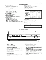
SPECIFICATIONS .............................................................................................................................................................  3
NAMES OF PARTS ...........................................................................................................................................................  3
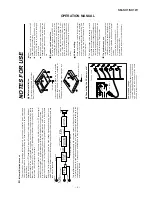
OPERATION MANUAL ....................................................................................................................................................... 5
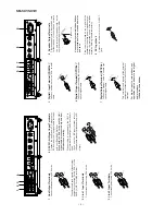
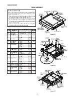
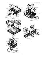
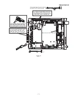
DISASSEMBLY ..................................................................................................................................................................  6
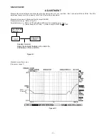
ADJUSTMENT ...................................................................................................................................................................  8
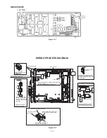
WIRING PROCESS DIAGRAM .......................................................................................................................................  10
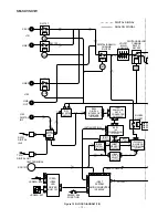
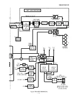
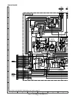
BLOCK DIAGRAM ...........................................................................................................................................................  12
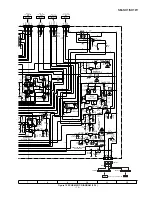
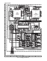
SCHEMATIC DIAGRAM / WIRING SIDE OF P.W.BOARD .............................................................................................. 14
NOTES ON SCHEMATIC DIAGRAM ..............................................................................................................................  32
TYPES OF TRANSISTOR AND DIODE ..........................................................................................................................  32
WAVEFORMS OF CD CIRCUIT ......................................................................................................................................  33
TROUBLESHOOTING .....................................................................................................................................................  34
FUNCTION TABLE OF IC ................................................................................................................................................  37
PARTS GUIDE/EXPLODED VIEW/PACKING OF PARTS (SM-SX1 FOR U.S.A. ONLY)

SACD

DIGITAL1 DIGITAL2

LINE1

LINE2

MODEL

1-BIT AMPLIFIER

SM-SX1W

MODEL

1-BIT AMPLIFIER

Summary of Contents for SM-SX1

Page 1: ...ge IMPORTANT SERVICE NOTES SM SX1 FOR U S A ONLY 2 AC POWER SUPPLY CORD SM SX1W ONLY 2 SPECIFICATIONS 3 NAMES OF PARTS 3 OPERATION MANUAL 5 DISASSEMBLY 6 ADJUSTMENT 8 WIRING PROCESS DIAGRAM 10 BLOCK DIAGRAM 12 SCHEMATIC DIAGRAM WIRING SIDE OF P W BOARD 14 NOTES ON SCHEMATIC DIAGRAM 32 TYPES OF TRANSISTOR AND DIODE 32 WAVEFORMS OF CD CIRCUIT 33 TROUBLESHOOTING 34 FUNCTION TABLE OF IC 37 PARTS GUIDE...

Page 2: ...hm 10 watt resistor paralleled by a 0 15µF capacitor in series with all exposed metal cabinet parts and a known earth ground such as conduit or electrical ground connected to earth ground Use a VTVM or VOM with 1000 ohm per volt or higher sensitivity to measure the AC voltage drop across the resistor See diagram Connect the resistor connection to all exposed metal parts having a return path to the...

Page 3: ...240 V 50 60 Hz Power source North America Australia New Zealand Singapore Hong Kong Other countries 51 W 55 W 55 W 55 W 55 W 55 W POWER CONSUMPTION POWER SOURCE Specifications for this model are subject to change without prior notice SPECIFICATIONS NAMES OF PARTS SACD DIGITAL1 DIGITAL2 LINE1 LINE2 3 2 4 1 4 Volume Control Knob Controls the sound level To cut the output to the speaker with the powe...

Page 4: ...ce If the volume is turned up too high with the speakers of less than 8 ohms impedance con nected the protection circuit of the amplifier activates Nothing is heard temporarily 9 AC Input Jack Connect the power cord to the AC INPUT jack Speaker cord 2 Line 1 Input Terminals Connect equipment using RCA cords 3 Line 2 Input Terminals Connect equipment using RCA cords 1 Line Output Terminals Connect ...

Page 5: ... AC outlet after any connections Unplug the AC power cord from the AC outlet if the unit will not be in use for a prolonged period of time Never use a power cord other than the one supplied Use of a power cord other than the one supplied may cause an electric shock or fire Speaker cord connection Be sure that the power is turned OFF when connecting the speaker cord Failure to turn the power off ca...

Page 6: ...t Right 2 Socket E2 x3 6 Front Bracket 1 Screw F1 x1 7 1 2 Nut F2 x1 3 Screw F3 x8 4 Socket F4 x1 7 Shield Cover A 1 Screw G1 x4 7 2 8 Shield Cover B 1 Screw H1 x4 7 2 9 Microcomputer 1 Socket J1 x2 7 3 PWB 2 PWB Holder J2 x4 10 Main PWB 1 Screw K1 x5 7 3 2 Socket K2 x5 11 Power PWB 1 Screw L1 x8 7 4 2 Screw L2 x2 3 Socket L3 x2 12 AC Input Filter 1 Screw M1 x1 7 4 PWB 2 PWB Holder M2 x3 13 Input ...

Page 7: ...2 x2 Microcomputer PWB Main PWB Push Push Microcomputer PWB Pull 1 2 Figure 7 3 Figure 7 5 Figure 7 2 Figure 7 1 Figure 7 4 F3 x4 ø3x6mm F3 x2 ø3x6mm F4 x1 F3 x2 ø3x6mm Front Bracket Power PWB Volume Bracket Volume Knob Washer Washer Power Knob F1 x1 ø3x8mm F2 x1 AC Input Filter PWB UNT501 502 Input Source PWB 1 Bit Amp PWB L1 x8 ø3x8mm L2 x2 ø3x6mm M1 x1 ø3x6mm N1 x1 ø3 x6mm L3 x2 M2 x3 P1 x4 AC ...

Page 8: ...asuring instrument Yokokawa Electric brand SA2400 Measurement range Refer to Fig 8 2 Adjustable range 1250Hz to 100kHz within 3dB from the standard noise curve 2 Noise strength of 125Hz Noise strength of 250Hz 20dB AC POWER SUPPLY UNIT Specterum Analyzer Speaker terminal Apply the analyzer between Lch and Lch and between Rch and Rch Figure 8 1 Standard noise floor curve Frequency range 1 Figure 8 ...

Page 9: ...gure 9 1 Check that the AC DC output voltage is 22V 0 15V at the A connector Ifdifferent adjustthevoltageusingthesemifixed VOL as described above Simplified offset voltage adjustment 1 It is fitted to the mechanical center of VRA1 VRA2 VRA3 and VRA4 FIg 10 1 2 Connect the digital multimeter to the terminals of the speaker and adjust the voltage between and of each terminal to 0 10 mVolt with VRA1 ...

Page 10: ...12Pconnectorfrom theterminalPWB MicrocomputerPWBCNP904 SeeFig A F i g B 30mm 30mm 5P Pull out the lead wires from above Press the lead wires wound around the core toward the SP relay PWB Press the core to the terminal board with the core stood core core F i g A Placethecorenearthe connector Twistthe12Pleadwireandwindit aroundcoreonce neartheconnector Mountthecoreandlockit Then insert theconnectors...

Page 11: ... 2P 2P After passing through the cores insert the terminals in the 4P and 6P housings Core Afterwindingtheleadwirearoundthecore insertthe7PconnectorfromtheSPrelay PWBintheterminalPWB Performthe abovebyplacingthecorearoundtheplace shown Becarefulnottotouchthescrew To avoid unnecessary radiation attach felt to each lead wire and fix it to the case in order that the lead wires do not overlap each oth...

Page 12: ... IC A B IC102 INVERTER 74HC153F IC103 BUFFER AMP 74HCT04F 1BIT TERMINAL RX101 DIGITAL IN 2 TX101 DIGITAL OUT SOC101 IC800 DIGITAL INTERFACE RECEIVER YM3436D IC801 SAMPLING RATE CONVERTER SM5844AF IC803 1bit CONVERSION TDA1307 IC806 CONTROL 74ACT00F IC811 TC7W74F IC802 TC7W04F IC807 SELECT 74ACT00F IC804 CLOCK SELECT 74ACT00F IC805 IC809 WAVEFORM RECTIFICATION 74HC74AF RLY800 RLY801 Q801 Q802 Q803 ...

Page 13: ...t 22V IC301 NJM431U REGULATOR 22V UNIT501 AC DC CONVERTER UNIT502 AC DC CONVERTER IC302 DC DC CONVERTER TZ0775AF IC306 NJM431U Q306 Q307 IC303 NJM78M05 12V 1bit Dig 5V Ana 5V 5V Digital RELAY SW MICROCOMPUTER 5V OP AMP 10V IC304 NJM78M12 10V IC304 NJM78M12 SW501 POWER LINE FILTER F501 SM SX1 4A 125V SM SX1W T3 15A L 250V SOC501 AC INLET SM SX1 AC120V 60Hz SM SX1W AC110 127 220 240V 50 60Hz ANALOG ...

Page 14: ...96 TP95 TP94 TP93 TP92 TP91 TP89 TP88 TP87 TP86 TP85 TP84 TP82 TP81 TP80 RLY301 C352 10 25 R305 27K R306 27K C346 47P R376 15K R301 1K C354 0 0047 BI302 R371 820 R373 1M C341 0 01 R303 2 7K CNP303 D301 DAN202K Q301 2SC2412KR C35 0 004 C347 0 0047 R341 10 C345 47P Q 2SA R345 4 7K R348 82K C348 0 0047 Q31 2SA103 D302 DAN202K CNP304 IC307 NJM4558M MOTOR DRIVE C337 0 01 C340 0 01 D323 DAN202K R347 4 7...

Page 15: ... C308 220 35 C2412KR C316 100 16 D307 1SR154 R314 22 C327 0 01 D311 1SR154 D310 1SR154 D313 1SR154 C353 0 0047 C347 0 0047 R319 1K C313 10 25 D305 1SR154 R355 100K 47P Q310 2SA1037KR R312 1K R391 2 2 R348 82K L302 220µH R379 15K Q315 2SA1036KR ZD304 HZ5BLL IC304 NJM78M12 C322 0 01 C315 100 16 ZD303 MTZJ5 6B R382 8 2K CNP304 IC307 NJM4558M MOTOR DRIVE C319 2200 35 C318 2200 35 C306 47 20 C307 0 01 ...

Page 16: ...CK 1CLR 14 13 12 11 10 9 8 7 6 5 4 3 2 1 NC NC VDD 2CLR 2D 2Q 2Q GND 2CK 1D 2PR 1Q 1Q 1PR 1CK 1CLR 11 14 13 12 10 9 8 7 6 5 4 3 2 1 NC VDD GND 12 14 13 11 10 9 8 7 6 5 4 3 2 1 CK VDD GND 12 14 13 11 10 9 8 7 6 5 4 3 2 1 GND VDD 8 7 6 5 4 3 2 1 NC PR CLR Q Q D CK GND VDD 5 4 3 2 1 5 4 3 2 1 MUTE D CNT RAB CL DA DDIN 37 36 R R L TO MICROCOMPUTER PWB P23 12 F IC810 PC CONTROLL IC812 INVERTER IC802 IN...

Page 17: ... GND D Protect Protect B 24V DDIN 5V D 7 6 5 4 3 2 1 5 4 3 2 1 GND D A GND DR DL DL GND D A 10V A GND A 10V A 10V A GND A L ch A R ch A 10V 37 36 12 9 R R L 5 4 DIGITAL PWB A2 TROLL IC802 INVERTER C809 WAVEFORM RECTIFICATION FROM MAIN PWB P14 1 F FROM INPUT SOURCE PWB P20 4 G R851 1K RLY802 C843 2 2 C836 47 10 TP38 R832 100 IC801 SM5844AF SAMPLING RATE CONVERTER C844 2 2 R843 100 R842 220 R841 220...

Page 18: ...1 SM1XP2 DA15 SM1XP2 ZDA7 HZU12B3 ZDA3 HZU12B3 HZU H DA16 SM1XP2 ZDA8 HZU12B3 DA12 SM1XP2 ZDA4 HZU12B3 HZ HZU DA14 SM1XP2 DA13 SM1XP2 CA41 1 0 CA47 1 0 RA59 10 DA9 SM1XP2 CA43 1 0 RA53 10 RA57 10 CA45 1 0 RA55 10 DA10 SM1XP2 CA40 1 0 CA42 1 0 RA60 10 CA46 1 0 CA44 1 0 RA54 10 RA56 10 RA58 10 RA7 75K RA5 75K RA8 75K RA6 75K CA7 0 22 CA5 10 63 CA6 10 63 C 0 RA2 10K RA86 100K RA85 100K CNPA3 CNPA1 CN...

Page 19: ...3 820 RA61 820 VRA1 200 RA62 820 VRA2 200 RA101 6 8K RA103 6 8K RA102 6 8K RA104 6 8K BLA4 CA50 100 50 CA51 100 50 BLA19 BLA22 BLA20 BLA23 BLA18 BLA21 BLA25 BLA24 CA52 100 50 LA806 5 6µH QA9 MP4712 QA10 MP4712 DA11 SM1XP2 DA15 SM1XP2 DA7 U12B3 ZDA3 HZU12B3 ZDA1 HZU12B3 ZDA5 HZU12B3 DA16 SM1XP2 ZDA8 HZU12B3 DA12 SM1XP2 A4 12B3 ZDA2 HZU12B3 ZDA6 HZU12B3 BLA6 CA13 100 10 BLA5 BLA3 CA14 100 10 BLA1 BL...

Page 20: ... C131 0 0015 L123 100µH TP58 TP59 TP51 TP50 TP49 TP48 TP47 TP46 TP45 TP44 BI102 TO DIGITAL PWB TP52 TP53 TP54 TP55 TP56 TP57 TP60 TP61 TP62 TP63 TP20 TP19 TP18 TP17 TP16 TP15 TP14 TP13 TP12 TP11 TP10 TP7 TP9 TP8 TP6 TP5 TP4 TP3 TP2 TP1 C103 0 001 C126 0 0015 C101 0 001 C124 0 0015 L110 L113 L127 J102 J102 LINE OUT LINE1 J101 LINE2 SACD L109 L126 D103 DAN202K R111 4 7K R110 4 7K R106 4 7K R105 4 7K...

Page 21: ... 4 3 2 1 7 6 5 4 3 2 1 CNP904 TO MICROCOMPUTER PWB P22 5 E A B C D 6 1 6 SPEAKER RELAY PWB A3 L201 L202 L203 L204 L205 L206 L207 BI201 TO INPUT SOURCE PWB TP82 TP81 TP80 TP79 TP78 TP77 TP76 C122 0 022 C129 0 68 C128 0 0015 C131 0 0015 L123 100µH L122 100µH TP72 TP73 TP74 TP75 TP71 TP70 TP69 TP68 SPEAKER TERMINAL TP61 TP62 TP63 TP64 TP65 TP66 TP67 TP43 TP42 TP41 TP40 TP39 TP38 TP37 TP35 TP34 TP33 T...

Page 22: ...SM SX1W AC110 127 220 240V 50 60Hz TO MAIN PWB P15 12 H Put The Plastic Inner Tube TP976 TP977 TP975 TP974 TP973 TP972 TP970 TP969 TP968 TP967 TP968 TP969 TP970 LED904 PX1124AF LED901 PX1124AF LED900 PX1124AF LED902 LNG91LCF LED903 LNG91LCF R904 100 R901 100 R900 100 R902 100 R903 100 R913 100 R910 100 R909 100 R911 100 R912 100 R975 3 6k R905 3 9K R906 5 6K R907 12K R908 39K CNP900 SW900 DIGITAL ...

Page 23: ... 5 6 7 8 KEYC KEYB KEYA VOL DIS KEY IC CLK DATA_OUT DATA_IN 23 CL_CONT COMPUTER PWB A8 B B B B B B B B B B B B B 8 7 6 5 4 3 2 1 10 11 12 13 14 15 16 17 18 10 1 8 5 4 2 3 CNS903 CNS902 R950 1K R946 1K CNP902 CNP903 IC908 PST9119 RESET C901 10 16 R923 10K D900 DAN202K X900 8 0MHz CNP901 R929 1K R926 1K R925 1K R918 1K R919 1K R920 1K R921 1K R922 1K R955 1K R956 1K R957 1K R958 1K R951 1K R952 1K R...

Page 24: ... 1 CNP302 R307 ZD304 CNP306 D304 L303 R390 L301 CNP305 CNP304 CNP303 BI302 RLY301 RLY302 Q323 Q321 Q324 Q322 C335 Q325 Q327 Q328 Q326 C336 C316 C323 C317 C351 C352 C324 ZD303 L302 Q307 R397 R396 IC304 IC305 C344 C325 C326 C304 Q304 C315 ZD302 Q306 R391 D324 IC302 Q309 R392 C331 D325 C306 C314 C309 C313 D306 R393 ZD301 THY301 C308 IC303 RLY303 C318 C319 BI301 C334 C333 1 2 3 4 3 2 1 3 2 1 3 2 1 1 2...

Page 25: ... R381 R348 R349 Q319 R367 R363 R371 R369 C349 C339C338 IC307 R361 C345 C347 R359 R380 R374 Q316 Q314 R376 R372 R378 C354 Q320 C350 R358 C348 4 5 8 1 8 5 4 1 MAIN PWB A1 BOTTOM UNT502 UNT501 CNWS504 CNWS505 TO POWER PWB P30 4 A O POWER PWB P30 5 A BR COLOR TABLE RD R OR YL GR BL VL GY WH W BK PK BROWN RED ORANGE YELLOW GREEN BLUE VIOLET GRAY WHITE BLACK PINK Through hole where the top and bottom pa...

Page 26: ...29 TP1 TP31 C815 TP2 TP34 R813 R818 L811 TP33 TP36 R821 TP35 R802 R800 R809 R810 R811 R801 R803 TP38 L800 C831 C802 R825 L813 L812 C827 C828 L805 R822 L803 C818 C817 C820 R824 R815 R868 R808 R807 R814 C810 R806 C807 R865 C806 C812 C805 TP8 R864 C809 TP9 TP6 L105 L126 R114 L110 R105 R113 D103 R125 R119 R212 D203 R202 R210 Q206 TP119 4 3 2 1 8 7 6 5 9 10 11 12 13 14 15 RLY802 RLY800 CNP801 C813 C834...

Page 27: ...3 R862 IC807 IC802 C826 C829 R827 C840 R832 R869 R870 R817 R816 R820 R819 C816 C850 R866 IC811 IC803 R201 R203 R867 C847 IC812 C851 C849 IC810 C846 IC800 X800 IC801 C841 7 5 8 1 14 10 L121 9 16 1 8 5 15 10 8 14 7 1 1 7 14 8 8 14 7 1 8 14 7 1 5 8 1 4 7 1 1 1 8 14 44 44 34 34 33 33 23 23 22 22 12 12 11 11 15 15 20 20 25 25 30 30 35 35 40 40 5 5 10 10 1 4 5 8 8 5 1 4 8 5 1 4 BR COLOR TABLE RD R OR YL...

Page 28: ...CK31 RA81 RA82 CK2 RA5 RA6 CK29 CA85 CA86 CK24 CK30 RA83 RA84 CK33 CK5 CK23 CK4 RA85 RA86 CK22 CK10 BIA4 CK11 CK12 CK13 CK35 CK14 CK15 CK16 CK20 CK21 RA58 RA54 RA56 ZDA4 ZDA2 CA46 CA40 CA44 RA102 CK5 CK1 CNPA3 CNPA1 CNPA2 CNPA4 CA52 CA51 BLA2 BLA3 BLA4 BLA6 BLA25 BLA23 BLA22 BLA21 BLA5 BLA24 BLA20 BLA1 CNPA5 BLA19 BLA18 CA50 DA11 DA9 DA13 DA15 DA16 DA14 DA10 DA12 QA9 QA10 LA803 LA804 LA801 LA802 L...

Page 29: ...3 24 13 20 15 1 5 10 12 7 7 8 8 10 10 14 14 1 1 5 5 1 1 1 1 8 8 8 8 5 5 5 5 4 4 4 4 1BIT PWB B BOTTOM BR COLOR TABLE RD R OR YL GR BL VL GY WH W BK PK BROWN RED ORANGE YELLOW GREEN BLUE VIOLET GRAY WHITE BLACK PINK Through hole where the top and bottom patterns are connected Through hole where the top bottom and B patterns are connected Through hole where the top bottom and ground patterns are con...

Page 30: ... 7 8 9 6 10 2 3 4 5 1 7 8 9 6 10 2 3 4 5 1 7 8 9 6 10 1 8 5 4 3 2 1 12 11 10 9 8 7 6 5 4 3 2 1 11 10 9 8 7 6 5 4 3 2 1 8 7 6 5 4 3 2 1 C909 IC902 IC901 IC900 BI900 C901 C903 L900 X900 CNP901 CNP903 CNP904 CNP902 LED904 LED903 LED902 LED901 LED900 CNP900 C503 CNP502 C530 L501 C502 L502 CNP501 R501 C501 CNP503 SW501 1 2 3 4 5 6 7 8 CNS901 SW501 POWER SW902 SACD SW900 DIGITAL1 SW901 DIGITAL2 SW903 LI...

Page 31: ...906 IC904 IC903 IC905 R970 R968 R969 R967 1 9 5 15 10 18 10 9 1 18 15 5 23 33 34 35 30 25 20 15 12 22 11 10 5 1 44 40 1 3 5 4 L901 L902 L903 SEGMENT PWB A5 BOTTOM SELECT SWITCH PWB A7 BOTTOM MICROCOMPUTER PWB A 8 BOTTOM AC INPUT FILTER PWB A6 BOTTOM 18 1 9 10 15 5 BR COLOR TABLE RD R OR YL GR BL VL GY WH W BK PK BROWN RED ORANGE YELLOW GREEN BLUE VIOLET GRAY WHITE BLACK PINK Through hole where the...

Page 32: ...means 1000 kohm and the resistor without any symbol is ohm type resistor Besides the one with Fusible is a fuse type Capacitor To indicate the unit of capacitor a symbol P is used this symbol P means pico farad and the unit of the capacitor without such a symbol is microfarad As to electrolytic capacitor the expression capacitance withstand voltage is used CH TH RH UJ Temperature compensation ML M...

Page 33: ...erve each pair OUTR OUTL OUTR OUTL RA5 RA7 RA6 RA8 Observe each pair QA1 QA5 QA2 QA6 QA3 QA7 QA4 QA8 RA5 RA6 RA7 RA8 QA2 QA1 3 4 BASE QA6 QA5 7 8 BASE 7 8 6 Observe Lo and Hi of ICA4 to 7 of each Lo Hi Observe SW section of Lch and Rch of each Observe each pair QA9 QA11 QA10 QA12 QA13 QA15 QA14 QA16 QA10 QA9 13 14 GATE QA12 QA11 15 16 GATE Set 22V at GND for observation of 6 to 8 Figure 33 1 Figur...

Page 34: ...ied and LED904 is lit Check whether 12V is supplied to RLY201 and RLY202 or not Check the surroundings of Q201 Q202 R201 to R202 Check whether Q203 and Q204 are on or not Check the line Q203 and Q204 from Pin 41 of the microcomputer IC907 Are they properly wired to the 1 bit amplifying unit CNWAM1 CNWAM2 CNWAM3 CNWAM4 No Yes Is voltage properly supplied to 1 bit amplifier CNP306 Check whether the ...

Page 35: ...k the line amplifying circuit Yes Is any signal output from CNP108 Yes Check the wiring to 1 bit amplifying unit and 1 bit amplifying unit No No sound on the digital input alone Yes Is 5V supplied to Pin 8 of CNS800 Check IC303 No Yes Is any digital signal output from Pin 9 of IC102 Check IC102 No Yes Is any digital signal output from Pin 8 of IC103 Check the wiring of CNS800 and CNP800 Check IC10...

Page 36: ...lating circuit No Are the waveforms of QA1 to QA8 correct Fig 33 3 Fig 33 4 Fig 33 5 Check ICA2 ICA3 QA1 to QA7 Yes No Are the waveforms of ICA4 to ICA7 correct Fig 33 6 Check ICA4 to ICA7 Yes No Are the waveforms of QA9 to QA16 correct Fig 33 7 Fig 33 8 Check RA53 to FA60 and QA9 to QA16 Yes No Is any signal output from CNWAM6 and CNWAM7 Check LA802 to LA808 Check the soldering Yes Check the surr...

Page 37: ...usual connect it to VSSA 29 VSSA Grand VCO system Externally connect it to VSS 30 TSTN Input LSI test terminal As usual it is not connected 31 KM2 Input Clock mode selection 2 H PLL synchronization L XI synchronization 32 KM0 Input Clock mode selection 0 H EXTW input L DDIN input 33 FS1 Output Sampling frequency code output 1 channel status output 34 FS0 Output Sampling frequency code output 0 use...

Page 38: ...0 VDDA VSSA PCO CTLP CTLN LR LOCKN P256 KM2 XI XO KM1 SKSY VDD VSS 36 37 35 40 41 43 44 42 1 18 19 2 20 21 3 4 17 30 23 5 10 16 39 11 22 13 12 31 14 15 38 25 28 26 29 24 32 1 2 3 4 5 6 7 8 9 10 11 12 13 14 15 16 17 18 19 20 21 22 33 32 31 30 29 28 27 26 25 24 23 44 43 42 41 40 39 38 37 36 35 34 DAUX HDLT DOUT VFL OPT SYNC MCC WC MCB MCA SKSY XI XO P256 LOCKN VSS TST2 DIM1 DIM0 DOM1 DOM0 KM1 FS1 KM...

Page 39: ... resistor 25 26 IISN Input with pull up resistor IIS output mode selection H Normal mode L IIS mode 27 STATE Output Output to express the internal operational state for operation check 28 TST1N Input with pull up resistor Control of output dither H Dither OFF L Dither ON 29 TST2N Input with pull up resistor Test terminal Set at H 30 31 RSTN Input with pull up resistor Reset terminal 32 33 VSS GND ...

Page 40: ...44AF 2 2 Note 1 fsi means the word clock LRCI on the input side and fso means the work clock LRCO on the output side Note 2 When H level is set open is also applicable Note 3 When the terminal of plural terminal Nos For the same terminal name is used it does not matter whether either or both terminals are connected Figure 40 BLOCK DIAGRAM OF IC MCOM MDT FSI1 MCK FSI2 MLEN DEEM ICLK ICKSL LRCI RSTN...

Page 41: ...utput Digital silence detected active LOW on left channel 12 DSR Output Digital silence detected active LOW on right channel 13 DSTB Input Note 2 DOBM stand by mode enforce pin active HIGH 14 CLC1 Input Application mode programming pin for CDEC pin 7 frequency division 15 CMIC Output Clock output provided to be used as running clock by microprocessor in master mode only output 96fs 16 VSS3 Ground ...

Page 42: ...LING 3rd 4th ORDER NOISE SHAPER 27 28 35 34 33 26 DOL NDOL CDAC NDOR DOR MODE BITSTREAM DATA OUTPUTS MICROPROCESSOR INTERFACE DA 38 CL 39 RAB 42 POR 20 VDD3 8 VDD1 21 VDDOSC 24 VDDAL 29 VDDAR 32 VDD2 41 DSR 12 DSL 11 TEST1 36 TEST2 37 19 RESYNC 10 DOBM 13 DSTB 5 SBCL 6 SBDA CRYSTAL OSCIL LATOR 25 VSSOSC 22 XTAL1 23 XTAL2 15 CMIC 7 CDEC 14 CLC1 17 CLC2 18 CDCC 9 VSS2 16 VSS3 30 VSSAL 31 VSSAR 40 VS...

Page 43: ... the latch output appears as it is However the output Qn is L when the latch output is H and Qn is hi Z when the latch output is L 6 RST Input Shift register latch reset 7 9 GND 0V Power supply 10 O8 Output Latch output at 8th step of shift register 11 O7 Output Latch output at 7th step of shift register 12 O6 Output Latch output at 6th step of shift register 13 O5 Output Latch output at 5th step ...

Page 44: ...ock output 25 P13 TMIO3 DLATCH Output Setting output to D A Latch output 26 P14 TMIO4 DDATA Input Output Setting output to D A Data input output 27 P20 IRQ0 PROTECT Input PROTECT signal detection input 28 P21 IRQ1 SENS P IN Input Warning input 29 P22 IRQ2 IC_STB Input External IC communication strobe 30 P60 DIG_B Output Digital input switch B Switch of digital input is controlled with DIG_A and B ...

Page 45: ... CLK CL_CONT VDD OSC2 OSC1 VSS SDATA SLATCH SCLK IC_RESET AUD MUTE Pin No Terminal Name Function 1 VDD Positive Supply to lower gate drivers De couple this pin to Vss pin 7 Bootstrap diode connected to HB pin 2 2 HB High Side Bootstrap supply External bootstrap capacitor is required Connect positive side of bootstrap capacitor to this pin Bootstrap diode is on chip 3 MO High Side Output Connect to...

Page 46: ...l for AD converter 17 L CH IN Input L channel analog input terminal 18 L CH Vref Reference voltage terminal for L channel 19 R CH Vref Reference voltage terminal for R channel 20 R CH IN Input R channel analog input terminal 21 RESET Input Reset terminal It is reset with L 22 NFR2 Input R channel reverse signal feedback input terminal 23 NFR1 Input R channel forward signal feedback input terminal ...

Page 47: ... Square type without lead wire VC J The 13th character represents capacity difference J 5 K 10 M 20 N 30 C 0 25 pF D 0 5 pF Z 80 20 If there are no indications for the electrolytic capacitors error is 20 Resistors VRD Carbon film type VRS Carbon film type VRN Metal film type VR MF Cylindrical type without lead wire VR MN Cylindrical type without lead wire VR TV Square type without lead wire VR TQ ...

Page 48: ...DDAN202K 1 J AB Silicon DAN202K D324 327 VHD1SR154 4 1 J AC Silicon 1SR154 D328 VHDDAN202K 1 J AB Silicon DAN202K D800 803 VHDDAN202K 1 J AB Silicon DAN202K D900 VHDDAN202K 1 J AB Silicon DAN202K DA1 8 VHD1SS355 1 J AB Silicon 1SS355 DA9 16 VHDSM1XP2 1 J AD Silicon SM1XP2 LED900 904 RH PX1124AFZZ J AL LED White PX1124AF LED905 907 VHPGL9BC030 1 J BA LED White GL9BC030 ZD101 VHEMTZJ5R1B 1 J AC Zene...

Page 49: ...39 RC KZ1255AFZZ J AD 0 22 µF 100V Ceramic CA40 43 RC KZ1252AFZZ J AE 1 µF 50V Ceramic CA44 45 RC KZ1253AFZZ J AF 1 µF 100V Ceramic CA46 47 RC KZ1252AFZZ J AE 1 µF 50V Ceramic CA50 RC EZ1698AFZZ J AD 100 µF 50V Electrolytic CA51 52 VCEAVA1HN107M J AC 100 µF 50V Electrolytic CA81 86 RC KZ1218AFZZ J AD 2 2 µF 10V CA801 804 RC FZ1139AFZZ J AF 0 56 µF 250V Electrolytic CA805 810 RC FZ1137AFZZ J AE 0 2...

Page 50: ...AQ100D J AA 10 ohm 1 10W RA61 64 VRN TV2AS821D J AA 820 ohms 1 10W RA70 71 VRN TV2AS203D J AA 20 kohms 1 10W RA81 86 VRN TV2AS104D J AA 100 kohm 1 10W RA91 94 VRN TV2AS682D J AA 6 8 kohms 1 10W RA101 104 RR DZ1126AFZZ J AC 6 8 kohms 4W RA801 804 RR SZ1063AFZZ J AC 16 ohms 3W OTHER CIRCUITRY PARTS BI101 CNS704 QCNWN6855AFZZ J AM Connector Ass y 12 12Pin BI102 CNS800 QCNWN6856AFZZ J AL Connector Ass...

Page 51: ...et Insulation B Except for SM SX1 280 PSHEZ1202AFZZ J AH Sheet Shield 281 PSHEM0152AFZZ J Tape Earth 282 QCNWN6926AFZZ J AB Lug Wire 283 PSHEM0151AFZZ J Sheet Cover 284 PSHEG0203AFZZ J AP Sheet Sound Absorbing 285 PSHEP0429AFZZ J AE Sheet Insulator C 286 PSHEZ1204AFZZ J Sheet Shield B 289 TSPC 3992AFSA J AF Label Specifications SM SX1 For U S A Canada 289 TSPC 3993AFSA J Label Specifications SM SX...

Page 52: ...PWB A1 9 DCEKL0784AF03 J Main Digital Speaker Relay Input Source Segment AC Input Filter Select Switch Micromputer Power Combined Ass y SM SX1 PWB A1 9 DCEKL0784AF06 J Main Digital Speaker Relay Input Source Segment AC Input Filter Select Switch Micromputer Power Combined Ass y For SM SX1W PWB B DCEKM0388AF03 J 1 Bit AMP 5 ...

Page 53: ...with 239 240 241 248 293 289 290 248 291 249 250 251 253 254 256 257 258 259 261x2 SOC501 261 262 262 266 267 267 268 268 269 269 269 269 270 270 280 283 282 281 207 624x5 625x10 619x2 636 625x10 623x3 621 616x5 602x8 602x4 601x2 621x2 621x2 607x2 621x2 623x3 610x5 609x4 607x2 621x2 630 608 611 631 629 602x2 206 with 220 221 PWB A9 PWB A2 PWB A7 PWB A5 PWB A3 ...

Page 54: ...52 255 255 255 260 263 264 265 265 264 272 278 284 285 286 257x2 257x2 257 257 257 257x2 210 257 257 211 x6 213x3 216x2 602x4 602 635 636 627 613x4 617x2 613x2 632 618 628 620x4 628 632 602 618 604 604 604 614 612 601 604 601 602x5 602 616x2 605x2 606x2 601x2 602x7 602x5 602x2 601x5 602x2 604 604x2 604 620x4 602x4 618x5 PWB A8 PWB A6 PWB A4 PWB B PWB A1 210 279 QA10 QA9 IC303 Q309 Q304 257 295 295...

Page 55: ...thylene Bag Accessories Operation Manual Warranty Card Leg Cushion SPAKZ0562AFZZ Pad Top Rear SPAKZ0554AFZZ Pad Protect SPAKA2756AFZZ Packing Add Left SPAKA2755AFZZ Packing Add Right SPAKZ0555AFZZ Pad Front SPAKC7117AFZZ Packing Case Bar Cord Label Home Page Address Label Home Page Address Label SSAKH0330AFZZ Sheet Unit SPAKZ0546AFZZ Leg Protection Material ...

Page 56: ...stem or transmitted in any from or by any means electronic mechanical photocopying recording or otherwise without prior written permission of the publisher A0007 184DS HA J SC SL LAG SA SZ EX SPC SRH SHARP CORPORATION Communication Systems Group Quality Reliability Control Center Higashihiroshima Hiroshima 739 0192 Japan Printed in Japan ...

Reviews: