S H A R I =
SERVICE
MANUEL DE SERVICE
l
l
l
Page
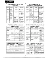
SPECIFICATIONS . . . . . . . . . . . . . . . . . .
NAMES OF PARTS . . . . . . . . . . . . . . . .
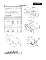
DISASSEMBLY . . . . . . . . . . . . . . . . . . .
VOLTAGE SELECTION. . . . . . . . . . . . . .
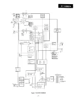
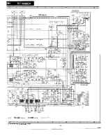
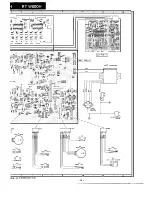
BLOCK DIAGRAM . . . . . . . . . . . . . . . . . . . . 7
NOTES ON SCHEMATIC DIAGRAM . . . . . . . . . 8
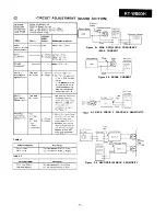
CIRCUIT ADJUSTMENT . . . . . . . . . . . . 9,
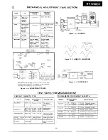
MECHANICAL ADJUSTMENT . . . . . . . . . . . .
l
l
l
Page
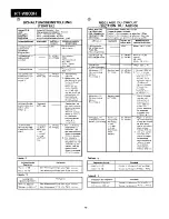
TYPES OF TRANSISTORS AND LED . . . . . . .
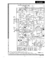
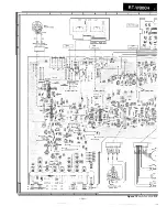
S C H E M A T I C D I A G R A M
. . . . . . . . . . . . . .
W I R I N G S I D E O F
. . . . . . . . .
E Q U I V A L E N T C I R C U I T ( B L O C K D I A G R A M
O F
. . . . . . . . . . . . . . . . . . . . . . . . . . . . . .
19
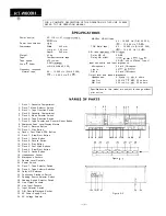
EXPLODED VIEW
. . . . . . . . . . . . . . . . . . . . .
REPLACEMENT PARTS LIST . . . . . . . . . . . .
Saite
DATEN . . . . . . . . . . . . . . . . 2-4
DER
. . . . . . . . . .
ZERLEGEN . . . . . . . . . . . . . . . . . . . . . . . . . ...5.6
SPANNUNGSWAHL . . . . . . . . . . . . . . . . . .
BLOCKSCHALTPLAN . . . . . . . . . . . . . . . 7
A N M E R K U N G E N Z U M
SCHALTPLAN
8
M E C H A N
. . . . . . . . . .
. . . . .
NOMENCLATURE . . . . . .
.
R E M A R Q U E S C O N C E R N A N T L E
D I A G R A M M E
D U
. .
D E
.
Page
. .
2 - 4
.
2 - 4
. .
. . .
. .
7
8
1: 12
Seite
. . . . . . . . . . . . . . . . . . . . .
S C H A L T P L A N
. . . . . . .
VERDRAHTUNSSEITE DER
. . . . . . . . . . . . . . . . . .
S C H A L T P L A N ) D E S
. . . . . . . . . . . . . . . . . . . . . .
19
. . . . . . . . . . . . .
. . . . . . . . . . . . . . . . . . . .
Page
TYPES DE TRANSISTOR ET LED
. . . . . . . . .
D I A G R A M M E
. . . . . . . . . .
D E L A P L A Q U E T T E D E
M O N T A G E
. . . . . . . . . . . . . .
C I R C U I T S E Q U I V A L E N T S ( D I A G R A M M E
D E C l . . . . . . . . . . . . . . . . . . .
19
. . . . . . . . . . . . . . . . . . . . .
DES
D E R E C H A N G E . . . . . . .
SHARP CORPORATION
Summary of Contents for RT-W800H
Page 7: ...Figure 7 BLOCK DIAGRAM 7 ...
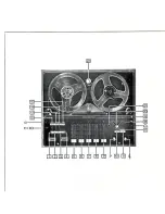
Page 15: ...I H 1 I 2 I 3 4 5 I 6 I I i f I I I I I 1 I 2 I 3 I 4 I il I Figure 15 WYRING SIDE OF 15 ...
Page 16: ...I 7 I a I 9 I 10 I 11 I 12 f JACK PWS A3 I 7 I a I 9 I 10 I 11 I 12 I D E OF P W BOARD l 2 16 ...
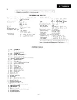
Page 19: ...I I 0 I n I m I 0 I 0 I W I D n L I I G I n I m I u I 0 I W I D ...
Page 20: ...2 I 31 606X41 w I 1 A 336 A ...