


PZ-MR2T
PZ-43MR2U
PZ-50MR2U
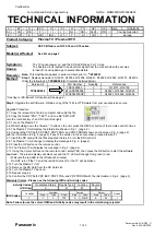
SERVICE MANUAL
S12F4PZ50MR2U
In the interests of user-safety (Required by safety regulations in some countries) the set should be restored
to its original condition and only parts identical to those specified should be used.
MODELS
PZ-MR2T
PZ-43MR2U
PZ-50MR2U
CONTENTS
Page
PLASMA DISPLAY TV
(AVC SYSTEM)
»
IMPORTANT SERVICE SAFETY PRECAUTION ..... 2
»
SPECIFICATIONS ................................................ 4
»
OPERATION MANUAL ........................................ 5
»
DIMENSIONS .................................................... 13
»
REMOVING OF MAJOR PARTS ....................... 14
»
ADJUSTMENT PROCEDURES ......................... 16
»
DESCRIPTION OF MAJOR IC FUNCTIONS .... 22
»
TROUBLE SHOOTING TABLE .......................... 49
»
PRINTED WIRING BOARD BLOCK DIAGRAM .. 56
»
SYSTEM BLOCK DIAGRAM ............................. 58
Page
»
SIGNAL FLOW BLOCK DIAGRAM .................... 60
»
DC/DC CONVERTER BLOCK DIAGRAM ......... 62
»
POWER BLOCK DIAGRAM ............................... 64
»
PC I/F BLOCK DIAGRAM .................................. 66
»
OVERALL WIRING DIAGRAM ........................... 68
»
DESCRIPTION OF SCHEMATIC DIAGRAM ..... 72
»
WAVEFORMS .................................................... 73
»
SCHEMATIC DIAGRAM ..................................... 74
»
PRINTED WIRING BOARD ASSEMBLIES ...... 114
»
PARTS LIST ..................................................... 121
»
PACKING OF THE SET ................................... 145
SHARP CORPORATION
This document has been published to be used for
after sales service only.
The contents are subject to change without notice.
Summary of Contents for PZ-43MR2U
Page 13: ...13 PZ MR2T PZ 43MR2U PZ 50MR2U Dimensions Unit mm ...
Page 36: ...36 PZ MR2T PZ 43MR2U PZ 50MR2U Ë VHiTA1318AF 1 ASSY IC604 Sync Processor Block Diagram ...
Page 38: ...38 PZ MR2T PZ 43MR2U PZ 50MR2U Ë VHiPD64082 1S ASSY IC7001 Y C Separate IC Block Diagram ...
Page 40: ...40 PZ MR2T PZ 43MR2U PZ 50MR2U Ë VHiCXD2093Q 1 ASSY IC402 Digital Comb Filter Block Diagram ...
Page 63: ...63 17 16 19 18 15 14 13 12 11 10 PZ MR2T PZ 43MR2U PZ 50MR2U ...
Page 64: ...64 8 7 10 9 6 5 4 3 2 1 A B C D E F G H PZ MR2T PZ 43MR2U PZ 50MR2U POWER BLOCK DIAGRAM ...
Page 65: ...65 17 16 19 18 15 14 13 12 11 10 PZ MR2T PZ 43MR2U PZ 50MR2U ...
Page 71: ...71 17 16 19 18 15 14 13 12 11 10 PZ MR2T PZ 43MR2U PZ 50MR2U ...
Page 74: ...74 8 7 10 9 6 5 4 3 2 1 A B C D E F G H PZ MR2T PZ 43MR2U PZ 50MR2U Ë MAIN UNIT 1 7 ...
Page 75: ...75 17 16 19 18 15 14 13 12 11 10 PZ MR2T PZ 43MR2U PZ 50MR2U ...
Page 76: ...76 8 7 10 9 6 5 4 3 2 1 A B C D E F G H PZ MR2T PZ 43MR2U PZ 50MR2U Ë MAIN UNIT 2 7 ...
Page 77: ...77 17 16 19 18 15 14 13 12 11 10 PZ MR2T PZ 43MR2U PZ 50MR2U ...
Page 78: ...78 8 7 10 9 6 5 4 3 2 1 A B C D E F G H PZ MR2T PZ 43MR2U PZ 50MR2U Ë MAIN UNIT 3 7 ...
Page 79: ...79 17 16 19 18 15 14 13 12 11 10 PZ MR2T PZ 43MR2U PZ 50MR2U ...
Page 80: ...80 8 7 10 9 6 5 4 3 2 1 A B C D E F G H PZ MR2T PZ 43MR2U PZ 50MR2U Ë MAIN UNIT 4 7 ...
Page 81: ...81 17 16 19 18 15 14 13 12 11 10 PZ MR2T PZ 43MR2U PZ 50MR2U ...
Page 82: ...82 8 7 10 9 6 5 4 3 2 1 A B C D E F G H PZ MR2T PZ 43MR2U PZ 50MR2U Ë MAIN UNIT 5 7 ...
Page 83: ...83 17 16 19 18 15 14 13 12 11 10 PZ MR2T PZ 43MR2U PZ 50MR2U ...
Page 84: ...84 8 7 10 9 6 5 4 3 2 1 A B C D E F G H PZ MR2T PZ 43MR2U PZ 50MR2U Ë MAIN UNIT 6 7 ...
Page 85: ...85 17 16 19 18 15 14 13 12 11 10 PZ MR2T PZ 43MR2U PZ 50MR2U ...
Page 86: ...86 8 7 10 9 6 5 4 3 2 1 A B C D E F G H PZ MR2T PZ 43MR2U PZ 50MR2U Ë MAIN UNIT 7 7 ...
Page 87: ...87 17 16 19 18 15 14 13 12 11 10 PZ MR2T PZ 43MR2U PZ 50MR2U ...
Page 88: ...88 8 7 10 9 6 5 4 3 2 1 A B C D E F G H PZ MR2T PZ 43MR2U PZ 50MR2U Ë FRONT UNIT ...
Page 89: ...89 17 16 19 18 15 14 13 12 11 10 PZ MR2T PZ 43MR2U PZ 50MR2U ...
Page 90: ...90 8 7 10 9 6 5 4 3 2 1 A B C D E F G H PZ MR2T PZ 43MR2U PZ 50MR2U Ë AV UNIT 1 3 ...
Page 91: ...91 17 16 19 18 15 14 13 12 11 10 PZ MR2T PZ 43MR2U PZ 50MR2U ...
Page 92: ...92 8 7 10 9 6 5 4 3 2 1 A B C D E F G H PZ MR2T PZ 43MR2U PZ 50MR2U Ë AV UNIT 2 3 ...
Page 93: ...93 17 16 19 18 15 14 13 12 11 10 PZ MR2T PZ 43MR2U PZ 50MR2U ...
Page 94: ...94 6 5 4 3 2 1 A B C D E F G H PZ MR2T PZ 43MR2U PZ 50MR2U Ë AV UNIT 3 3 ...
Page 95: ...95 6 5 4 3 2 1 A B C D E F G H PZ MR2T PZ 43MR2U PZ 50MR2U Ë LED Unit ...
Page 96: ...96 8 7 10 9 6 5 4 3 2 1 A B C D E F G H PZ MR2T PZ 43MR2U PZ 50MR2U Ë SR Unit ...
Page 97: ...97 17 16 19 18 15 14 13 12 11 10 PZ MR2T PZ 43MR2U PZ 50MR2U ...
Page 98: ...98 8 7 10 9 6 5 4 3 2 1 A B C D E F G H PZ MR2T PZ 43MR2U PZ 50MR2U Ë PC I F Unit 1 7 ...
Page 99: ...99 17 16 19 18 15 14 13 12 11 10 PZ MR2T PZ 43MR2U PZ 50MR2U ...
Page 100: ...100 8 7 10 9 6 5 4 3 2 1 A B C D E F G H PZ MR2T PZ 43MR2U PZ 50MR2U Ë PC I F Unit 2 7 ...
Page 101: ...101 17 16 19 18 15 14 13 12 11 10 PZ MR2T PZ 43MR2U PZ 50MR2U ...
Page 102: ...102 8 7 10 9 6 5 4 3 2 1 A B C D E F G H PZ MR2T PZ 43MR2U PZ 50MR2U Ë PC I F Unit 3 7 ...
Page 103: ...103 17 16 19 18 15 14 13 12 11 10 PZ MR2T PZ 43MR2U PZ 50MR2U ...
Page 104: ...104 8 7 10 9 6 5 4 3 2 1 A B C D E F G H PZ MR2T PZ 43MR2U PZ 50MR2U Ë PC I F Unit 4 7 ...
Page 105: ...105 17 16 19 18 15 14 13 12 11 10 PZ MR2T PZ 43MR2U PZ 50MR2U ...
Page 106: ...106 8 7 10 9 6 5 4 3 2 1 A B C D E F G H PZ MR2T PZ 43MR2U PZ 50MR2U Ë PC I F Unit 5 7 ...
Page 107: ...107 17 16 19 18 15 14 13 12 11 10 PZ MR2T PZ 43MR2U PZ 50MR2U ...
Page 108: ...108 8 7 10 9 6 5 4 3 2 1 A B C D E F G H PZ MR2T PZ 43MR2U PZ 50MR2U Ë PC I F Unit 6 7 ...
Page 109: ...109 17 16 19 18 15 14 13 12 11 10 PZ MR2T PZ 43MR2U PZ 50MR2U ...
Page 110: ...110 8 7 10 9 6 5 4 3 2 1 A B C D E F G H PZ MR2T PZ 43MR2U PZ 50MR2U Ë PC I F Unit 7 7 ...
Page 111: ...111 17 16 19 18 15 14 13 12 11 10 PZ MR2T PZ 43MR2U PZ 50MR2U ...
Page 112: ...112 8 7 10 9 6 5 4 3 2 1 A B C D E F G H PZ MR2T PZ 43MR2U PZ 50MR2U Ë POWER and EMC Unit ...
Page 113: ...113 17 16 19 18 15 14 13 12 11 10 PZ MR2T PZ 43MR2U PZ 50MR2U ...
Page 115: ...115 6 5 4 3 2 1 A B C D E F G H PZ MR2T PZ 43MR2U PZ 50MR2U MAIN Unit B Side ...
Page 116: ...116 6 5 4 3 2 1 A B C D E F G H PZ MR2T PZ 43MR2U PZ 50MR2U PC I F Unit A Side ...
Page 117: ...117 6 5 4 3 2 1 A B C D E F G H PZ MR2T PZ 43MR2U PZ 50MR2U PC I F Unit B Side ...
Page 120: ...120 6 5 4 3 2 1 A B C D E F G H PZ MR2T PZ 43MR2U PZ 50MR2U AV Unit Component Side ...