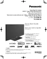
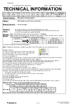
background image

PZ-43MR2E
PZ-50MR2E

SERVICE MANUAL

  S12E6PZ50MR2E

In the interests of user-safety (Required by safety regulations in some countries) the set should be restored
to its original condition and only parts identical to those specified should be used.

CONTENTS

Page

SHARP CORPORATION

PLASMA DISPLAY TV

(AVC SYSTEM)

»

IMPORTANT SERVICE SAFETY PRECAUTION ..... 2

»

SPECIFICATIONS ................................................ 3

»

OPERATION MANUAL ........................................ 4

»

DIMENSIONS .................................................... 11

»

REMOVING OF MAJOR PARTS ........................ 12

»

ADJUSTMENT PROCEDURES ......................... 14

»

DESCRIPTION OF MAJOR IC FUNCTIONS .... 20

»

TROUBLE SHOOTING TABLE .......................... 43

»

PRINTED WIRING BOARD BLOCK DIAGRAM .. 50

»

SYSTEM BLOCK DIAGRAM ............................. 52

»

SIGNAL FLOW BLOCK DIAGRAM .................... 54

Page

»

DC/DC CONVERTER BLOCK DIAGRAM ......... 56

»

POWER BLOCK DIAGRAM ............................... 58

»

PC I/F BLOCK DIAGRAM .................................. 60

»

OVERALL WIRING DIAGRAM ........................... 62

»

DESCRIPTION OF SCHEMATIC DIAGRAM ..... 66

»

WAVEFORMS .................................................... 67

»

SCHEMATIC DIAGRAM ..................................... 68

»

PRINTED WIRING BOARD ASSEMBLIES ...... 108

»

PARTS LIST ..................................................... 115

»

PACKING OF THE SET ................................... 139

MODELS

PZ-43MR2E
PZ-50MR2E

Summary of Contents for PZ-43MR2E

Page 1: ... 2 SPECIFICATIONS 3 OPERATION MANUAL 4 DIMENSIONS 11 REMOVING OF MAJOR PARTS 12 ADJUSTMENT PROCEDURES 14 DESCRIPTION OF MAJOR IC FUNCTIONS 20 TROUBLE SHOOTING TABLE 43 PRINTED WIRING BOARD BLOCK DIAGRAM 50 SYSTEM BLOCK DIAGRAM 52 SIGNAL FLOW BLOCK DIAGRAM 54 Page DC DC CONVERTER BLOCK DIAGRAM 56 POWER BLOCK DIAGRAM 58 PC I F BLOCK DIAGRAM 60 OVERALL WIRING DIAGRAM 62 DESCRIPTION OF SCHEMATIC DIAGR...

Page 2: ... servicing BEFORE RETURNING THE RECEIVER Fire Shock Hazard Before returning the receiver to the user perform the following safety checks 1 Inspect all lead dress to make certain that leads are not pinched and check that hardware is not lodged between the chassis and other metal parts in the receiver 2 Inspect all protective devices such as non metallic control knobs insulation materials cabinet ba...

Page 3: ...UT 2 SCART AV in out S VIDEO in AV Link INPUT 3 SCART AV in out S VIDEO in RGB in Component ANTENNA 75 q Din Type for VHF UHF in INPUT 4 S VIDEO AV in PC INPUT 15 Pin mini D Sub Audio in Audio Variable Fixed S VIDEO out AV out Power Requirement AC 220 240 V 50 60 Hz 40 W 0 8 W Standby Dimensions 430 W 70 H 330 D mm Weight 4 4 kg Accessories Power cord Remote control unit Two AA size batteries Syst...

Page 4: ...ppear to be operating correctly it may need resetting In this case press CLEAR on the front of the unit as shown in the diagram Press CLEAR lightly with the end of a ballpoint pen or other pointed object This will reset the System as shown below AV MODE resets to STANDARD TV channel resets to channel 1 Dual screen resets to normal Audio setting initialises SRS resets to Off Image position is initi...

Page 5: ...screen 13 C CHANNEL INFORMATION Display the channel information and time 14 b INPUT SOURCE Select an input source TV INPUT 1 INPUT 2 INPUT 3 INPUT 4 PC 15 SLEEP Set the SLEEP TIMER 16 e MUTE Mute the sound 17 0 9 TV External input mode Set the channel TELETEXT mode Set the page 18 o Digit for channel select Change the digits of the selected TV channel 19 Colour RED GREEN YELLOW BLUE TELETEXT mode ...

Page 6: ... power cord to the AVC System L TO PREVENT RISK OF ELECTRIC SHOCK DO NOT TOUCH UN INSULATED PARTS OF ANY CABLES WITH THE POWER CORD CONNECTED Speaker cables GRAYeGRAY with white stripe Speaker cable Speaker cable As you apply pressure to this part insert the speaker cable It is important to match polarity when connecting the speaker cables to the terminals Insert the speaker cable Lift up the snap...

Page 7: ...uded with the system for cable management Follow the diagram below for correct cable management System cable Wedge the power cord and the system cable into the groove on the stand Power cord Speaker cable Stick the speaker cable clamps 2 4 to the surface as shown System cable clamp Speaker cable clamp Speaker cable clamp System cable System cable clamp ...

Page 8: ...he battery cover Cautions regarding batteries Improper use of batteries can result in chemical leakage or explosion Be sure to follow the instructions below Do not use manganese batteries When you replace the batteries use alkaline ones Place the batteries with their terminals corresponding to the e and f indications Do not mix batteries of different types Different types of batteries have differe...

Page 9: ...y TV like a decoder VCR DVD player computer game console and camcorder To view external source images select the input source from b on the remote control unit or INPUT on the Plasma Display TV Panel Unit L To protect all equipment always turn off the AVC System before connecting to a decoder VCR DVD player computer game console camcorder or other external equipment The S video signal only outputs...

Page 10: ...th 6 Audio left input 7 Not used 8 Audio video control 9 Earth 10 AV LINK control 11 Not used 12 Not used 13 Earth 14 Not used 15 Chroma S Video input 16 Not used 17 Earth for video 18 Earth 19 Video output 20 Video input S video input 21 Plug shield SCART INPUT 3 1 Audio right output 2 Audio right input 3 Audio left output 4 Common earth for audio 5 Earth 6 Audio left input 7 Blue input 8 Audio v...

Page 11: ...11 PZ 43MR2E PZ 50MR2E Dimensions Unit mm ...

Page 12: ...m the system cable white terminal and the RS 232C terminal both on the PC I F unit 6 2 Remove two lock screws from the system cable gray terminal also on the SR unit 6 3 Remove the two lock screws from the PC I F unit bracket 6 4 Remove the four lock screws from the PC I F unit and SR unit assemblies Take out these assemblies 6 5 Remove the three lock screws from the brackets of the PC I F unit an...

Page 13: ...Remove the six lock screws from the AV unit and detach this unit 9 Remove the EMC unit assemblies 9 1 Remove the two lock screws from the EMC unit bracket 9 2 Remove the two lock screws from the EMC unit and detach this unit 10 Remove the three lock screws from the power unit and detach this unit ...

Page 14: ...lled to the AVC System using the cross cable for the RS 232C port for the details of the program see Appendix 3 Open the MS DOS window on the PC and then go to the directory in which the software is installed 4 Start up the system to which the AVC System and Panel Unit have been connected 5 Run vup bat tentaive name at the MS DOS prompt The software will be upgraded 6 Load the file civc_XXXXa bhxm...

Page 15: ...in the delivery adjustment mode become valid Description The user s adjustment parameters and others will be set to the default values The channel settings will also be initialized 4 Exiting a special mode 1 Process adjustment mode Press the PROCESS ADJ button located on the remote control unit or turn OFF the power 2 Inspection process mode Set the parameter SIGNAL INFO to 0 on page 6 or 7 of the...

Page 16: ...M Y level adjustment SECAM colour density level adjustment SECAM Cr level adjustment N358 Y level adjustment N358 colour density adjustment N358 Cr level adjustment N358 tone adjustment COMP 15 k Y level adjustment COMP 15 k colour density adjustment COMP 15 k Cr level adjustment COMP HDTV black level adjustment COMP HDTV Y level adjustment COMP HDTV colour density adjustment The values for the ab...

Page 17: ...ue 3 25 3 29 V 3 AVC center 2 5V adjustment Connect DC voltmeter to TP1701 Adjust output voltage of DC DC 2 5 V line to 2 6 V Adjusted value 2 60 2 64 V 1 Setup 1 Set colour system to PAL 2 Select PAL source 100 colour bar signal including 100 white such as split field colour bar Adjustment item Description Adjustment procedure 2 Tuner Y level adjustment 1 Adjust TP1101 so that the Y signal withou...

Page 18: ...AIN SECAM adjustment 1 Adjust TB1274_MAIN output TP801 to 0 35 0 025 Vp p 0 35V 0 35V 1 Setup 1 Set colour system to N358 2 Select N358 source 100 SMPTE colour bar or similar colour bar signal including 100 white Adjustment item Description Adjustment procedure 2 N358 Y CONTRAST adjustment 1 Adjust TB1274_MAIN output TP803 to 0 7 0 05 Vp p 3 N358 COLOR GAIN adjustment 1 Adjust TB1274_MAIN output T...

Page 19: ...al including 100 white like split field colour bar Adjustment item Description Adjustment procedure 2 COMP HDTV CONTRAST adjustment Turn off the PEAK ACL control Adjust the output TP815 of pin 11 of IC810 to have 1 1 0 05 Vp p from the pedestal level 1 DATA COPY 1 Using the adjustment key set ON in the DATA COPY line Wait until OFF is displayed instead Finally turn off the power to quit the proces...

Page 20: ...cuit a PAL NTSC SECAM automatic selection circuit The PAL M N clock signals at 4 43 and 8 58 MHz are internally generated for colour demodulation The PAL SECAM demodulation circuit uses a base band signal processing system with built in IH DL and is therefore adjustment free The IC801 IC802 has 4 lines for YC signal input 2 lines for RGB signal input and 2 lines for colour difference signal input ...

Page 21: ...to the PC I F Unit in the 2 screen mode The video signals analog Y Cb Cr from CN6 are input to IC310 The video signals input to this IC are converted into digital signals and then sent to IC25 IC25 IX3434CE This IC performs the I P conversion and scaling to match the digitalized video with the output resolution and also the data conversion It has two input lines V0 and V1 The V0 line is used to pr...

Page 22: ...Z 50MR2E The information shown in the list is basic information and may not correspond exactly to that shown in the schematic diagrams Ë VHiCXA2069Q 1 ASSY IC1301 S2 Compatible 7 Input 3 Ouput AV Switch Block Diagram ...

Page 23: ...l Video signal output terminal for luminance signal output Video signal output terminal for chrominance signal output Audio signal output terminal Used to detect C signal superimposed S2 compatible DC level 4 3 video signal when below 1 3V 4 3 letterbox signal when between 1 3V and 2 5V 16 9 image squeeze signal when above 2 5V To be pulled down to GDN at 100KΩ to produce 4 3 video signal when ope...

Page 24: ...24 PZ 43MR2E PZ 50MR2E Ë VHiMM1519XQ 1 IC1401 Component Input Video Switch Block Diagram ...

Page 25: ...EO 1 Y DGND GND VIDEO 2 Pb VIDEO 2 Pr VIDEO 3 Pb VIDEO 3 Pr TUNER Pb TUNER Pr VIDEO 1 Pb VIDEO 1 Pr VIDEO 2 SW VIDEO 3 SW MONO SW VIDEO 1 SW ADDRESS SDA SCL DVCC L3 OUT L2 OUT L1 OUT Pr OUT 3 Pb OUT 3 Y OUT 3 Pr OUT 2 Pb OUT 2 Y OUT 2 Pr OUT 1 Pb OUT 1 Y OUT 1 I I I I I I I I I I I I I I I I I I I I I I I I I I I O I O O O O O O O O O O O O Line input of D terminal Analog power supply 9V Y signal ...

Page 26: ...s that have 1 written to them are pulled high by the internal pull up resistors and in that state can be used as inputs Port 0 is a 8 bit open drain bi directional I O port Port 0 pins that have 1 written to them float in this state they can be used as high impedance inputs Port is a 8 bit bi directional multifunction I O port with internal pull up resistors Port 1 pins that have 1 written to them...

Page 27: ...nal ENE has an internal pull up resistor which switches automatically to non emulation mode if ENE is not connected STOP Emulation control line Driving a low level during the input phase freezes the real time relevant internal peripherals such as timers and interrupt controller Opcode Fetch Emulation control line A high level driven by the controller during output phase indicates the beginning of ...

Page 28: ...28 PZ 43MR2E PZ 50MR2E Ë RH iX3371CEZZ ASSY IC2501 Multi Standard Sound Processor Block Diagram ...

Page 29: ...t ADR data output ADR word strobe ADR clock Digital power supply 5V Digital ground I2S2 data input Not connected Power on reset Not connected Headphone out right Headphone out left Reference ground 2 Loudspeaker out right Loudspeaker out left Not connected Subwoofer output Not connected SCART 2 output right SCART 2 output left Reference ground 1 SCART 1 output right SCART 1 output left Volume capa...

Page 30: ...30 PZ 43MR2E PZ 50MR2E Ë VHiTB1274AF 1Q ASSY IC801 IC802 VIDEO CHROMA Processor Block Diagram ...

Page 31: ...g pulse outputs Output of sync input Y signal selected with Video SW SYNC HVCO block power supply DC5V standard I2C BUS SCL terminal I2C BUS SDA terminal Selector switch for main signal and RGB1 input signal YS3 input effective only when RGB1 ENB is set at enable in bus setting SYNC HVCO block grounding terminal Y1 Cb1 Cr1 signal input Y clamp filter to be connected Y Cb Cr signal output Selector ...

Page 32: ... Independent horizontal sync signal input terminal IN2 V Independent vertical sync signal input terminal IN2 line signal input terminal Selector line and sync processor line power terminal IN3 H Independent horizontal sync signal input terminal IN3 V Independent vertical sync signal input terminal IN3 line signal input terminal Selector line and sync processor line grounding terminal IN4 H Indepen...

Page 33: ...ade at 2 6Vp p with 100IRE white input RGB AKB sample and hold terminal Reference pulse to return to this terminal Peak ABL peak holding terminal Used to form LPF for ABL control signal ABL control signal input terminal YM1 YS1 control input terminal Input level to be of 3 values VM turning off function also available when YM and YS have reached their specified values Analog RGB1 signal input term...

Page 34: ...D SP_CP TMS HD3 VCC VD3 GND MODEA MODEB MODEC SELA GND VCC SELO HD2 VD2 HDS VDS US_VD GND US_HD TCK TEXT_VD TEXT_HD VCC GND PL_BLK TDO PLCP PL_HD PL_VD GND GCLK1 OE1 GCLRn OE2 GCLK2 VCC CNR_CP CNR_HBLK HD1 I O I O I O I O I O I O I O I O I O I O I O I O I O I O I O I O I O I O I O I O I O I O I O I O I O I O I O I I I I I O I O I O Ground Power supply 3 3V Ground Ground Power supply 3 3V Ground Po...

Page 35: ...35 PZ 43MR2E PZ 50MR2E Ë VHiTA1318AF 1 ASSY IC604 Sync Processor Block Diagram ...

Page 36: ...f the horizontal output is varied by the volyage at this pin Connect the ceramic oscillator for horizontal oscillator The VCC pin 9 0V DAC1 output pin When TEST mode VD or vertical sync signal to frequency counter circuit is output DAC2 output pin When TEST mode HD or composite sync signal to frequency counter circuit is output DAC3 output pin This pin is open collector system When TEST mode test ...

Page 37: ...37 PZ 43MR2E PZ 50MR2E Ë VHiCXD2064Q 1 ASSY IC402 IC405 Digital Comb Filter Block Diagram ...

Page 38: ...tween this pin and GND for obtaining the output D A converter analog grounding terminal D A converter terminal Y C ch D A converter output full scale setting terminal x16 resistance to be connected against D A converter output resistance R D A converter terminal Test terminal fixed at Low Digital power terminal 5 0V Digital grounding terminal Y C separation mode setting terminal MODE2 MOD1 L L Mos...

Page 39: ...n YIN VCC GND CIN YOUT VCCO CVOUT COUT I I O O O Luminance input 5V supply for filters and references Ground Chrominance input Chrominance output Composite video output 5V supply for output stages Luminance output Ë VHiML6428C1 1 ASSY IC404 IC407 Low Pass Video Filter IC Block Diagram ...

Page 40: ...r Bank A Sync must be provided at SYNC IN pin Unfiltered analog G or U channel input for Bank B Sync must be provided at SYNC IN pin Unfiltered analog B or V channel input for Bank A Sync must be provided at SYNC IN pin Unfiltered analog B or V channel input for Bank B Sync must be provided at SYNC IN pin Analog B or V channel output Analog G or U channel output 5V power supply for output buffers ...

Page 41: ...41 PZ 43MR2E PZ 50MR2E Ë VHiFA3675F 1 ASSY IC1702 6 channel DC DC Converter IC Block Diagram ...

Page 42: ...put to error amplifier Ch 1 output of error amplifier Ch 5 non inverting input to error amplifier Ch 5 inverting input to error amplifier Ch 5 output of error amplifier Ch 6 inverting input to error amplifier Ch 6 output of error amplifier Ch 3 non inverting input to error amplifier Ch 3 inverting input to error amplifier Ch 3 output of error amplifier Ch 4 non inverting input to error amplifier C...

Page 43: ...cted with the PDP and the set as well NO YES YES YES Is the impedance of the M 10V line as specified Measure the resistance between F1702 and GND NO NO YES Are there voltage fluctuations along the OVP line pin 12 of P1502 NO Check the M 10V line as well as its circuit parts YES Are the DC DC converter output lines and MOS FET Q1712 Q1716 Q1726 and Q1718 as specified NO Chekc the D_POW and B 2 5V_P...

Page 44: ...in of IC1301 AV SWITCH normal Pins 52 and 54 of IC1301 L R OUT1 Pins 43 and 45 of IC1301 L R OUT2 Pins 38 and 40 of IC1301 L R OUT3 NO No audio output SCART2 3 YES Is audio output available at each related pin of IC2501 MULTI SOUND PROCESSOR normal Pins 27 and 28 of IC2501 SC1 OUT L R YES Check the circuit between pins 27 and 28 of IC2501 and pins 3 and 1 of SCART2 3 as well as audio mute circuit ...

Page 45: ...signal input at pin 43 at pin 48 in NTSC system YES NO Check IC801 and its peripheral circuits YES Are there MAIN Y Cb Cr signal outputs at pins 21 22 and 23 of IC801 respectively NO Check IC802 and its peripheral circuits Are there SUB Y Cb Cr signal outputs at pins 21 22 and 23 of IC802 respectively YES NO Check the line between IC801 and IC803 YES Are there MAIN Y Cb Cr signal inputs at pins 69...

Page 46: ...nu screen Select INPUT3 RGB on menu selection screen Is RGB signal input available at pins 5 7 and 9 of IC1401 AV SWITCH Check the circuit between pins 15 11 and 7 of SCART3 and pins 5 7 and 9 of IC1401 NO YES NO YES No component picture Is INPUT3 COMPONENT selected on Input Select menu screen Select INPUT3 COMPONENT on menu selection screen Is component signal input available at pins 15 17 and 19...

Page 47: ...C signal output at pin 58 of IC1301 respectively Is SUB Y signal output available at pin 44 and SUB C signal output at pin 47 of IC1301 respectively Check IC1301 and peripheral circuits No external input picture INPUT4 AV No external input picture INPUT4 S IN No picture 5 NO Is video signal output available at pin 41 of IC1301 AV SWITCH NO Is Y signal output available at pin 39 and C signal output...

Page 48: ...604 and peripheral circuits YES NO Is HD2M VD2 output available at pins 9 and 4 of IC802 SUB VIDEO CHROMA YES Is video signal input available at pin 21 of IC1601 TELETEXT CPU Is TELETEXT compatible broadcast received or are signals from other TELETEXT compatible equipment received at video input terminal and is TELETEXT selected on remote controller Check the circuit between pin 56 of IC1301 and p...

Page 49: ...igital output of IC25 normal Check IC25 and its peripheral circuits No PC picture YES Is signal available at pins 21 22 24 25 27 28 30 and 31 of IC413 The signal is of high frequency a little less than 1GHz Pay due attention to it during observation Monitor problem is likely NO PC I F Unit CPCi 0056CE internal problem is likely No MAIN picture on single screen and dual screen No SUB picture on dua...

Page 50: ...RMINAL J1101 COMP IN MONI OUT TERMINAL IC1102 CONTROL J1102 MONITOR S OUT TELTEXT AV LINK CIRCUIT COMP AV SWITCH CIRCUIT ANALOG AV SWITCH CIRCUIT CN1 CONNECTOR CN7 CONNECTOR CN6 CONNECTOR IC25 CIVIC IC1 CPU IC310 A D CONV IC4 VIDEO MAIN PC A D CONV IC413 PANEL LINK IC319 SDRAM IC320 SDRAM CN9 CONNECTOR CN8 CONNECTOR IC7 REG IC8 REG CN5 RS 232C CN3 DISPLAY OUT 1 IC405 RS 323 RECIVER PANEL LINK OUTP...

Page 51: ... CONNECTOR IC1502 DAC IC801 MAIN VIDEO CHROMA IC604 SYNC SEP IC803 RGB DECODER P1502 CONNECTOR P901 ADJUSTING CONNECTOR P1702 CONNECTOR SC1502 CONNECTOR SC1501 CONNECTOR IC403 CONTROL IC406 CONTROL IC802 SUB VIDEO CHROMA SC1503 CONNECTOR IC402 SUB COMB FIL CHROMA IC405 MAIN COMB FIL CHROMA IC901 PLD SC1504 CONNECTOR POWER SUPPLY ...

Page 52: ...52 8 7 10 9 6 5 4 3 2 1 A B C D E F G H PZ 43MR2E PZ 50MR2E SYSTEM BLOCK DIAGRAM ...

Page 53: ...53 17 16 19 18 15 14 13 12 11 10 PZ 43MR2E PZ 50MR2E ...

Page 54: ...54 8 7 10 9 6 5 4 3 2 1 A B C D E F G H PZ 43MR2E PZ 50MR2E SIGNAL FLOW BLOCK DIAGRAM ...

Page 55: ...55 17 16 19 18 15 14 13 12 11 10 PZ 43MR2E PZ 50MR2E ...

Page 56: ...56 8 7 10 9 6 5 4 3 2 1 A B C D E F G H PZ 43MR2E PZ 50MR2E DC DC CONVERTER BLOCK DIAGRAM ...

Page 57: ...57 17 16 19 18 15 14 13 12 11 10 PZ 43MR2E PZ 50MR2E ...

Page 58: ...58 8 7 10 9 6 5 4 3 2 1 A B C D E F G H PZ 43MR2E PZ 50MR2E POWER BLOCK DIAGRAM ...

Page 59: ...59 17 16 19 18 15 14 13 12 11 10 PZ 43MR2E PZ 50MR2E ...

Page 60: ... B PFDINH VCOOUT 13 1 4 9 10 5 6 SUB _Y SUB_ Cb SUB_ Cr SUB_ HD 2 1 SUB _VD About 60MHz 12pin TO CONNECTOR PWB SDRAM 512Kx128bitx4 BANK 8 V0_HSYNC V0_VSYNC V0_CSYNC OV0_V V0_HSYNR OV0_HSYNR V0_PDEN OV0_PDEN V0_CLP OV0_CLP V0_HSYNC2 V0_VDCLK_I OV0_HSC2 OVCLK Max60MHz V0_RA 7 0 V0_RB 7 0 V0_GA 7 0 V0_GB 7 0 V0_BA 7 0 V0_BB 7 0 8 8 8 8 8 XPW R_SV V1_GA 7 0 V1_BA 7 0 V1_RA 7 0 8 8 8 OV1_VCKO 15M Hz V1...

Page 61: ... SMPOW 7 AN2 6 CCKM S1 15 FWMODEN PTD1 PTF0 FLAS HWP PTE1 FST ATUS FLWP FLASH 2Mx16bit IC27 LH28F320S3NS C S0 DRAM 1Mx16bit IC28 MSM51V18165D PTD6 16 HOTPLUG ACL_S IG 44 5 PTG2 KOUTEI CLR_ SW PTD4 DAC_DATA PTJ4 13 16 PTJ5 DAC_CLK 8 PTE3 ACL_SW 25 PTE2 RES_OUT3 PTE1 3 SRESET PTG1 15 AW_ DATA PTC4 1 TV_COL2 PTC0 2 TV_COL1 PTB2 26 HPMUTE 1 PTB0 24 LMUTE PTJ7 14 SH_ON PTA5 18 AWC S_R PTA3 17 AWC S_W 4...

Page 62: ...8 POWER UNIT FRONT UNIT MAI PC I F UNIT P3401 S S P1301 CN703 CN702 CN6 CN7 CN1 SC1502 SC1501 P1502 QCNW 6073 QCNW 6074CEZ QCNW 6081CEZZ QCNW 6077CEZZ QCNW 6080CEZZ QCNW 6083CEZZ QCNW 6084CEZZ LED UNIT P3001 QCNW 6078CEZZ SR UNIT P6000 P6001 OVERALL WIRING DIAGRAM 1 2 ...

Page 63: ...13 12 11 10 PZ 43MR2E PZ 50MR2E NT UNIT MAIN UNIT AV UNIT TUNER P3402 P1703 SC1503 SC1401 P1301 P2502 P2501 P2503 SC1402 SC1504 P1702 QCNW 6073CEZZ QCNW 6075CEZZ QCNW 6082CEZZ QCNW 6079CEZZ QCNW 6076CEZZ W 6074CEZZ 6081CEZZ ...

Page 64: ...64 8 7 10 9 6 5 4 3 2 1 A B C D E F G H PZ 43MR2E PZ 50MR2E OVERALL WIRING DIAGRAM 2 2 ...

Page 65: ...65 17 16 19 18 15 14 13 12 11 10 PZ 43MR2E PZ 50MR2E ...

Page 66: ...are measured from point indicated to chassis ground INDICATION OF RESISTOR CAPACITOR RESISTOR 1 The unit of resistance Ω is omitted K kΩ 1000 Ω M MΩ 2 All resistors are 5 unless otherwise noted J 5 F 1 D 0 5 3 All resistors are Carbon type unless otherwise noted C Solid W Cement S Oxide Film T Special N Metal Coating CAPACITOR 1 All capacitors are mF unless otherwise noted P pF mmF 2 All capacitor...

Page 67: ...500mV div H 10µsec div 4 IC801 1 pin V 200mV div H 10µsec div 5 IC803 TP801 V 200mV div H 20µsec div 6 IC803 TP802 V 200mV div H 20µsec div 7 IC803 TP803 V 200mV div H 20µsec div 8 IC803 31 pin V 1V div H 20µsec div 9 IC810 13 pin V 500mV div H 20µsec div 0 IC810 11 pin V 500mV div H 20µsec div q IC810 10 pin V 500mV div H 20µsec div ...

Page 68: ...68 8 7 10 9 6 5 4 3 2 1 A B C D E F G H PZ 43MR2E PZ 50MR2E Ë MAIN UNIT 1 6 ...

Page 69: ...69 17 16 19 18 15 14 13 12 11 10 PZ 43MR2E PZ 50MR2E ...

Page 70: ...70 8 7 10 9 6 5 4 3 2 1 A B C D E F G H PZ 43MR2E PZ 50MR2E Ë MAIN UNIT 2 6 ...

Page 71: ...71 17 16 19 18 15 14 13 12 11 10 PZ 43MR2E PZ 50MR2E ...

Page 72: ...72 8 7 10 9 6 5 4 3 2 1 A B C D E F G H PZ 43MR2E PZ 50MR2E Ë MAIN UNIT 3 6 ...

Page 73: ...73 17 16 19 18 15 14 13 12 11 10 PZ 43MR2E PZ 50MR2E ...

Page 74: ...74 8 7 10 9 6 5 4 3 2 1 A B C D E F G H PZ 43MR2E PZ 50MR2E Ë MAIN UNIT 4 6 ...

Page 75: ...75 17 16 19 18 15 14 13 12 11 10 PZ 43MR2E PZ 50MR2E ...

Page 76: ...76 8 7 10 9 6 5 4 3 2 1 A B C D E F G H PZ 43MR2E PZ 50MR2E Ë MAIN UNIT 5 6 ...

Page 77: ...77 17 16 19 18 15 14 13 12 11 10 PZ 43MR2E PZ 50MR2E ...

Page 78: ...78 8 7 10 9 6 5 4 3 2 1 A B C D E F G H PZ 43MR2E PZ 50MR2E Ë MAIN UNIT 6 6 ...

Page 79: ...79 17 16 19 18 15 14 13 12 11 10 PZ 43MR2E PZ 50MR2E ...

Page 80: ...80 8 7 10 9 6 5 4 3 2 1 A B C D E F G H PZ 43MR2E PZ 50MR2E Ë FRONT UNIT ...

Page 81: ...81 17 16 19 18 15 14 13 12 11 10 PZ 43MR2E PZ 50MR2E ...

Page 82: ...82 8 7 10 9 6 5 4 3 2 1 A B C D E F G H PZ 43MR2E PZ 50MR2E Ë AV UNIT 1 3 ...

Page 83: ...83 17 16 19 18 15 14 13 12 11 10 PZ 43MR2E PZ 50MR2E ...

Page 84: ...84 8 7 10 9 6 5 4 3 2 1 A B C D E F G H PZ 43MR2E PZ 50MR2E Ë AV UNIT 2 3 ...

Page 85: ...85 17 16 19 18 15 14 13 12 11 10 PZ 43MR2E PZ 50MR2E ...

Page 86: ...86 8 7 10 9 6 5 4 3 2 1 A B C D E F G H PZ 43MR2E PZ 50MR2E Ë AV UNIT 3 3 ...

Page 87: ...87 17 16 19 18 15 14 13 12 11 10 PZ 43MR2E PZ 50MR2E ...

Page 88: ...88 8 7 10 9 6 5 4 3 2 1 A B C D E F G H PZ 43MR2E PZ 50MR2E Ë SR Unit ...

Page 89: ...89 17 16 19 18 15 14 13 12 11 10 PZ 43MR2E PZ 50MR2E ...

Page 90: ...90 8 7 10 9 6 5 4 3 2 1 A B C D E F G H PZ 43MR2E PZ 50MR2E Ë LED Unit ...

Page 91: ...91 17 16 19 18 15 14 13 12 11 10 PZ 43MR2E PZ 50MR2E ...

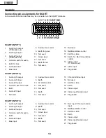
Page 92: ...92 8 7 10 9 6 5 4 3 2 1 A B C D E F G H PZ 43MR2E PZ 50MR2E Ë PC I F Unit 1 7 ...

Page 93: ...93 17 16 19 18 15 14 13 12 11 10 PZ 43MR2E PZ 50MR2E ...

Page 94: ...94 8 7 10 9 6 5 4 3 2 1 A B C D E F G H PZ 43MR2E PZ 50MR2E Ë PC I F Unit 2 7 ...

Page 95: ...95 17 16 19 18 15 14 13 12 11 10 PZ 43MR2E PZ 50MR2E ...

Page 96: ...96 8 7 10 9 6 5 4 3 2 1 A B C D E F G H PZ 43MR2E PZ 50MR2E Ë PC I F Unit 3 7 ...

Page 97: ...97 17 16 19 18 15 14 13 12 11 10 PZ 43MR2E PZ 50MR2E ...

Page 98: ...98 8 7 10 9 6 5 4 3 2 1 A B C D E F G H PZ 43MR2E PZ 50MR2E Ë PC I F Unit 4 7 ...

Page 99: ...99 17 16 19 18 15 14 13 12 11 10 PZ 43MR2E PZ 50MR2E ...

Page 100: ...100 8 7 10 9 6 5 4 3 2 1 A B C D E F G H PZ 43MR2E PZ 50MR2E Ë PC I F Unit 5 7 ...

Page 101: ...101 17 16 19 18 15 14 13 12 11 10 PZ 43MR2E PZ 50MR2E ...

Page 102: ...102 8 7 10 9 6 5 4 3 2 1 A B C D E F G H PZ 43MR2E PZ 50MR2E Ë PC I F Unit 6 7 ...

Page 103: ...103 17 16 19 18 15 14 13 12 11 10 PZ 43MR2E PZ 50MR2E ...

Page 104: ...104 8 7 10 9 6 5 4 3 2 1 A B C D E F G H PZ 43MR2E PZ 50MR2E Ë PC I F Unit 7 7 ...

Page 105: ...105 17 16 19 18 15 14 13 12 11 10 PZ 43MR2E PZ 50MR2E ...

Page 106: ...106 8 7 10 9 6 5 4 3 2 1 A B C D E F G H PZ 43MR2E PZ 50MR2E Ë POWER and EMC Unit ...

Page 107: ...107 17 16 19 18 15 14 13 12 11 10 PZ 43MR2E PZ 50MR2E ...

Page 108: ...6 5 4 3 2 1 A B C D E F G H 108 PZ 43MR2E PZ 50MR2E PRINTED WIRING BOARD DIAGRAM MAIN Unit A Side ...

Page 109: ...6 5 4 3 2 1 A B C D E F G H 109 PZ 43MR2E PZ 50MR2E MAIN Unit B Side ...

Page 110: ...6 5 4 3 2 1 A B C D E F G H 110 PZ 43MR2E PZ 50MR2E AV Unit Component Side ...

Page 111: ...6 5 4 3 2 1 A B C D E F G H 111 PZ 43MR2E PZ 50MR2E FRONT Unit Component Side SR Unit Component Side LED Unit Component Side ...

Page 112: ...6 5 4 3 2 1 A B C D E F G H 112 PZ 43MR2E PZ 50MR2E PC I F Unit A Side ...

Page 113: ...6 5 4 3 2 1 A B C D E F G H 113 PZ 43MR2E PZ 50MR2E PC I F Unit B Side ...

Page 114: ...6 5 4 3 2 1 A B C D E F G H 114 PZ 43MR2E PZ 50MR2E EMC Unit Component Side POWER Unit Component Side ...

Page 115: ... IC1504 VHiTC7W53U 1 J TC7W53FU AF IC1701 VHiFA3675F 1 J FA3675F AR IC1704 VHiBA09T FP 1 J BA09FP E2 AG IC1706 VHiBA08FP 1Y J BA08FP AF IC1708 VHiBA05FP 1Y J BA05FP AF IC1709 VHiBA05FP 1Y J BA05FP AF IC1710 VHiBA05FP 1Y J BA05FP AF IC1711 VHiBA05FP 1Y J BA05FP AF IC1712 VHiBA05FP 1Y J BA05FP AF IC1713 VHiBA12FP 1Y J I C AF IC1901 RH iX3566CEZZQ J I C AW IC1902 VHiM62320FP 1 J M62320FP AK IC1903 VH...

Page 116: ...J2R9N J Peaking 22µH AC L408 VP 1M220J2R9N J Peaking 22µH AC L409 VP 1M4R7J1R2N J Peaking 4 7µH AB L601 VP 1M120J1R9N J Peaking 12µH AC L602 VP 1M6R8J1R4N J Peaking 6 8µH AC L603 VP 1M470J5R4N J Peaking 47µH AC L604 VP 1M6R8J1R4N J Peaking 6 8µH AC L605 VP 1M5R6J1R2NY J Peaking 5 6µH AB L606 VP 1M8R2J1R5N J Peaking 8 2µH AC L607 VP 1M470J5R4N J Peaking 47µH AC L608 VP 1M3R9J1R0N J Peaking 3 9µH AC...

Page 117: ...KYCY1HB103K J 0 01 50V Ceramic AA C656 VCKYCY1EF104Z J 0 1 25V Ceramic AA C657 VCCCCY1HH181J J 180p 50V Ceramic AA C658 VCCCCY1HH221J J 220p 50V Ceramic AA C659 VCCCCY1HH221J J 220p 50V Ceramic AA C660 VCKYCY1HB103K J 0 01 50V Ceramic AA C661 VCKYCY1EF104Z J 0 1 25V Ceramic AA C662 VCKYCY1HB103K J 0 01 50V Ceramic AA C663 VCKYCY1EF104Z J 0 1 25V Ceramic AA C801 VCKYTV1EB104K J 0 1 25V Ceramic AB C...

Page 118: ...V Ceramic AB C1706 VCKYTV1CF105Z J 1 0 16V Ceramic AB C1707 VCKYTV1CF224Z J 0 22 16V Ceramic AB C1709 VCKYCY1EF104Z J 0 1 25V Ceramic AA C1711 VCKYTV1CF104Z J 0 1 16V Ceramic AA C1712 VCKYCY1EF104Z J 0 1 25V Ceramic AA C1713 VCKYCY1EF104Z J 0 1 25V Ceramic AA C1714 VCKYCY1HB222K J 2200p 50V Ceramic AA C1715 VCKYCY1HB222K J 2200p 50V Ceramic AA C1717 VCKYCY1CF334Z J 0 33 16V Ceramic AA C1718 VCEASM...

Page 119: ...R460 VRS CY1JF241F J 240 1 16W M Ox AA R461 VRS CY1JF391F J 390 1 16W M Ox AA R464 VRS CY1JF102F J 1 0k 1 16W M Ox AA R465 VRS CY1JF272F J 2 7k 1 16W M Ox AA R466 VRS CY1JF332F J 3 3k 1 16W M Ox AA R467 VRS CY1JF561J J 560 1 16W M Ox AA R468 VRS CY1JF563J J 56k 1 16W M Ox AA R469 VRS CY1JF391J J 390 1 16W M Ox AA R470 VRS CY1JF391J J 390 1 16W M Ox AA R471 VRS CY1JF391J J 390 1 16W M Ox AA R472 VR...

Page 120: ...VRS CY1JF103J J 10k 1 16W M Ox AA R820 VRS TQ2BD750J J 75 1 8W M Ox AA R821 VRS TQ2BD750J J 75 1 8W M Ox AA R822 VRS TQ2BD750J J 75 1 8W M Ox AA R829 VRS CY1JF681J J 680 1 16W M Ox AA R830 VRS CY1JF681J J 680 1 16W M Ox AA R831 VRS CY1JF471J J 470 1 16W M Ox AA R832 VRS CY1JF473F J 47k 1 16W M Ox AA R833 VRS CY1JF101J J 100 1 16W M Ox AA R834 VRS CY1JF101J J 100 1 16W M Ox AA R835 VRS CY1JF470J J ...

Page 121: ... Ox AA R1519 VRS CY1JF101J J 100 1 16W M Ox AA R1521 VRS CY1JF391J J 390 1 16W M Ox AA R1522 VRS CY1JF391J J 390 1 16W M Ox AA R1524 VRS CY1JF391J J 390 1 16W M Ox AA R1525 VRS CY1JF391J J 390 1 16W M Ox AA R1529 VRS CY1JF102J J 1 0k 1 16W M Ox AA R1530 VRS CY1JF472J J 4 7k 1 16W M Ox AA R1531 VRS CY1JF101J J 100 1 16W M Ox AA R1533 VRS CY1JF101J J 100 1 16W M Ox AA R1534 VRS CY1JF101J J 100 1 16W...

Page 122: ...401 RBLN 0061TAZZ J Ferrite Bead AD FB601 RBLN 0061TAZZ J Ferrite Bead AD FB602 RBLN 0061TAZZ J Ferrite Bead AD FB603 RBLN 0061TAZZ J Ferrite Bead AD FB801 RBLN 0061TAZZ J Ferrite Bead AD FB802 RBLN 0061TAZZ J Ferrite Bead AD FB803 RBLN 0061TAZZ J Ferrite Bead AD FB1701 RBLN 0210TAZZ J Ferrite Bead AB FB1702 RBLN 0210TAZZ J Ferrite Bead AB FB1703 RBLN 0210TAZZ J Ferrite Bead AB FB1704 RBLN 0210TAZ...

Page 123: ...1JF562J J 5 6k 1 16W M Ox AA R3404 VRS CY1JF103J J 10k 1 16W M Ox AA R3405 VRS TQ2BD561J J 560 1 8W M Ox AA R3406 VRS CY1JF101J J 100 1 16W M Ox AA R3407 VRS CY1JF562J J 5 6k 1 16W M Ox AA R3408 VRS CY1JF103J J 10k 1 16W M Ox AA R3409 VRS TQ2BD561J J 560 1 8W M Ox AA R3410 VRS CY1JF101J J 100 1 16W M Ox AA R3411 VRS CY1JF562J J 5 6k 1 16W M Ox AA R3412 VRS CY1JF103J J 10k 1 16W M Ox AA R3413 VRS C...

Page 124: ...1530AR 1 J 2SA1530AR AB Q1407 VS2SA1530AR 1 J 2SA1530AR AB Q1408 VS2SC3928AR 1Y J 2SC3928AR AB Q1409 VS2SC3928AR 1Y J 2SC3928AR AB Q1410 VS2SC3928AR 1Y J 2SC3928AR AB Q1411 VS2SC3928AR 1Y J 2SC3928AR AB Q1601 VS2SC3928AR 1Y J 2SC3928AR AB Q1602 VS2SC3928AR 1Y J 2SC3928AR AB Q1604 VS2SC3928AR 1Y J 2SC3928AR AB Q1605 VS2SA1530AR 1 J 2SA1530AR AB Q1606 VS2SC3928AR 1Y J 2SC3928AR AB Q1607 VS2SA1530AR ...

Page 125: ...B471K J 470p 50V Ceramic AA C1140 VCKYCY1HB471K J 470p 50V Ceramic AA C1141 VCKYTV1CB105K J 1 0 16V Ceramic AC C1142 VCKYTV1CB105K J 1 0 16V Ceramic AC C1143 VCKYTV1CB105K J 1 0 16V Ceramic AC C1144 VCKYTV1CB105K J 1 0 16V Ceramic AC C1145 VCCCCY1HH101J J 100p 50V Ceramic AA C1146 VCKYTV1CB105K J 1 0 16V Ceramic AC C1147 VCCCCY1HH100D J 10p 50V Ceramic AA C1148 VCKYCY1HB221K J 220p 50V Ceramic AA ...

Page 126: ... 0 1 25V Ceramic AA C1621 VCKYCY1EF104Z J 0 1 25V Ceramic AA C1622 VCKYCY1EF104Z J 0 1 25V Ceramic AA C1623 VCE9PF0JW226M J 22 6 3V EL N P AD C1624 VCKYCY1EF104Z J 0 1 25V Ceramic AA C1625 VCKYCY1EF104Z J 0 1 25V Ceramic AA C1626 VCKYCY1EF104Z J 0 1 25V Ceramic AA C1627 VCKYTV1CB105K J 1 0 16V Ceramic AC C1628 VCKYCY1EF104Z J 0 1 25V Ceramic AA C1629 VCKYCY1EF104Z J 0 1 25V Ceramic AA C1630 VCKYCY...

Page 127: ... 16W M Ox AA R1191 VRS CY1JF222J J 2 2k 1 16W M Ox AA R1192 VRS TW2ED750J J 75 1 4W M Ox AA R1193 VRS TW2ED750J J 75 1 4W M Ox AA R1194 VRS TW2ED750J J 75 1 4W M Ox AA R1195 VRS TV1JD221J J 220 1 16W M Ox AA R1196 VRS TV1JD221J J 220 1 16W M Ox AA R1197 VRS CY1JF104J J 100k 1 16W M Ox AA R1198 VRS CY1JF104J J 100k 1 16W M Ox AA R1199 VRS CY1JF101J J 100 1 16W M Ox AA R1200 VRS CY1JF101J J 100 1 16...

Page 128: ...1JF101J J 100 1 16W M Ox AA R1409 VRS CY1JF101J J 100 1 16W M Ox AA R1411 VRS CY1JF220J J 22 1 16W M Ox AA R1412 VRS CY1JF220J J 22 1 16W M Ox AA R1413 VRS CY1JF220J J 22 1 16W M Ox AA R1414 VRS CY1JF102J J 1 0k 1 16W M Ox AA R1415 VRS CY1JF102J J 1 0k 1 16W M Ox AA R1418 VRS CY1JF103J J 10k 1 16W M Ox AA R1421 VRS CA1JF101J J 100 1 16W M Ox AA R1422 VRS CY1JF100J J 10 1 16W M Ox AA R1423 VRS CY1J...

Page 129: ... 16W M Ox AA R2548 VRS CY1JF103J J 10k 1 16W M Ox AA SWITCH SW1601 QSW C0049CEZZ J Switch AF MISCELLANEOUS PARTS FB1101 RBLN 0051TAZZ J Ferrite Bead AC FB1102 RBLN 0051TAZZ J Ferrite Bead AC FB1103 RBLN 0051TAZZ J Ferrite Bead AC FB1104 RBLN 0062TAZZ J Ferrite Bead AB FB1105 RBLN 0077TAZZ J Ferrite Bead AB FB1106 RBLN 0051TAZZ J Ferrite Bead AC FB1107 RBLN 0051TAZZ J Ferrite Bead AC FB1108 RBLN 00...

Page 130: ...R6014 VRS TQ2BD000J J 0 1 8W M Ox AA R6020 VRS CY1JF472J J 4 7k 1 16W M Ox AA R6030 VRS CY1JF104J J 100k 1 16W M Ox AA R6031 VRS CY1JF104J J 100k 1 16W M Ox AA R6032 VRS CY1JF102J J 1k 1 16W M Ox AA R6033 VRS CY1JF102J J 1k 1 16W M Ox AA R6036 VRS CY1JF223J J 22k 1 16W M Ox AA R6037 VRS CY1JF103J J 10k 1 16W M Ox AA R6038 VRS CY1JF103J J 10k 1 16W M Ox AA R6039 VRS CY1JF681J J 680 1 16W M Ox AA R6...

Page 131: ...AC D53 9DK001 30001 J Diode 1SS193 AC D54 9DK001 30022 J Diode MA3120WA AG D55 9DK001 30022 J Diode MA3120WA AG D56 9DK001 30022 J Diode MA3120WA AG D57 9DK001 30022 J Diode MA3120WA AG D70 9DK001 30020 J Diode 1SS355 AD D71 9DK001 30020 J Diode 1SS355 AD D72 9DK001 30020 J Diode 1SS355 AD D73 9DK001 30021 J Diode 1SS400 AE D75 9DK001 30018 J Diode 1SS187 AD D76 9DK001 30018 J Diode 1SS187 AD D77 ...

Page 132: ...0V Ceramic AC C537 9DK001 40077 J 10 16V EL AF C538 9DK001 42094 J 0 1 25V Ceramic AC C542 9DK001 40077 J 10 16V EL AF C543 9DK001 42094 J 0 1 25V Ceramic AC C544 9DK001 42102 J 2200p 50V Ceramic AC C545 9DK001 42102 J 2200p 50V Ceramic AC C546 9DK001 42102 J 2200p 50V Ceramic AC C550 9DK001 40077 J 10 16V EL AF C551 9DK001 42094 J 0 1 25V Ceramic AC C552 9DK001 42094 J 0 1 25V Ceramic AC C553 9DK...

Page 133: ...eramic AC C886 9DK001 42152 J 0 47 16V Ceramic AC C887 9DK001 42151 J 120p 50V Ceramic AC C888 9DK001 42151 J 120p 50V Ceramic AC C889 9DK001 42151 J 120p 50V Ceramic AC C890 9DK001 40077 J 10 16V EL AF C891 9DK001 40077 J 10 16V EL AF C894 9DK001 42094 J 0 1 25V Ceramic AC C895 9DK001 42094 J 0 1 25V Ceramic AC C896 9DK001 42094 J 0 1 25V Ceramic AC C897 9DK001 42094 J 0 1 25V Ceramic AC C898 9DK...

Page 134: ...40 J 68 1 16W Resistor Array AD R960 9DK001 51040 J 68 1 16W Resistor Array AD R961 9DK001 51040 J 68 1 16W Resistor Array AD R962 9DK001 51040 J 68 1 16W Resistor Array AD R963 9DK001 51040 J 68 1 16W Resistor Array AD R964 9DK001 51040 J 68 1 16W Resistor Array AD R965 9DK001 51040 J 68 1 16W Resistor Array AD R966 9DK001 51040 J 68 1 16W Resistor Array AD R967 9DK001 51040 J 68 1 16W Resistor A...

Page 135: ... 13 pin AH CPCi 0056CE11 PC I F UNIT Continued INTEGRATED CIRCUITS IC701 VHiNJM2375AD1 J NJM2375AD AL IC702 VHiTNY264P 1 J TNY264P AN IC703 VHiTA76431S15 J TA76431 AF TRANSISTORS Q701 VS2SK2662 1 J 2SK2662 AH Q702 VS2SC1741AS 1 J 2SC1741AS AC Q703 VS2SK2700 1 J 2SK2700 AM Q704 VS2SC1741AS 1 J 2SC1741AS AC Q705 VSDTD113ZS 1 J DTD113ZS AD Q706 VSDTC124ESA 1 J DTC124ESA AC Q707 VSDTA124XSA 1 J DTA124...

Page 136: ...01J J 100 1 4W Carbon AA R724 VRD HT2EY471J J 470 1 4W Carbon AA R725 VRD HT2EY102J J 1k 1 4W Carbon AA R726 VRD HT2EY122J J 1 2k 1 4W Carbon AA R727 VRD HT2HY152J J 1 5k 1 2W Carbon AA R728 VRD HT2EY100J J 10 1 4W Carbon AA R729 VRD HT2EY101J J 100 1 4W Carbon AA R730 VRD HT2EY221J J 220 1 4W Carbon AA R731 VRD HT2EY102J J 1k 1 4W Carbon AA R732 VRD HT2EY103J J 10k 1 4W Carbon AA R733 VRNHT2EK360...

Page 137: ...2 6 2 13 SR Unit PC I F Unit EMC Unit 22 5 1 5 2 5 3 5 4 13 32 31 11 5 22 12 23 Main Unit AV Unit Front Unit Power Unit LED Unit 25 8 20 9 23 23 1 3 1 1 1 18 22 14 15 19 26 4 33 22 17 16 7 21 21 3 3 29 22 3 1 3 3 2 21 22 22 1 4 30 27 28 18 2 13 26 2 1 2 22 1 7 1 2 6 1 6 2 18 2 8 2 11 2 9 2 14 2 4 2 5 2 1 2 2 2 10 2 7 2 8 2 13 2 13 2 3 1 5 10 11 ...

Page 138: ...12 QCNW 6078CEZZ J Connecting Cord AM SR PC I F 13 QCNW 6080CEZZ J Connecting Cord AL MAIN PC I F 14 QCNW 6081CEZZ J Connecting Cord AD MAIN AV 15 QCNW 6082CEZZ J Connecting Cord AC MAIN AV 16 QCNW 6083CEZZ J Connecting Cord AD MAIN PC I F 17 QCNW 6084CEZZ J Connecting Cord AD MAIN PC I F 18 QEARZ0056CEFW J Earth Spring x6 AC 19 QEARZ0057CEFW J Earth Spring x1 AB 20 TLABN0428CEZZ J Serial No Label...

Page 139: ...RMCG1676CESA Buffer Material SPAKX2077CEZZ Packing Material SPAKF0515CEZZ Polyethylene Bag SSAKH0173CEZZ Polyethylene Bag SSAKA0170CEZZ FRONT Operation Manual PZ 43MR2E TiNS 7622CEZZ TiNS 7645CEZZ Operation Manual PZ 50MR2E TiNS 7520CEZZ TiNS 7631CEZZ Batteries AC Cord for UK QACCBA008WJZZ AC Cord for Europe QACCVA002WJZZ System Cable QCNW 6117CEZZ ...

Page 140: ... in a retrieval system or transmitted in any form or by any means electronic mechanical photocopying recording or otherwise without prior written permission of the publisher SHARP CORPORATION AV Systems Group Quality Reliability Control Center Yaita Tochigi 329 2193 Japan D JAPAN P JAPAN TQ1296 S Apr 2002 Printed in Japan SY KG ...

Reviews: