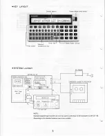
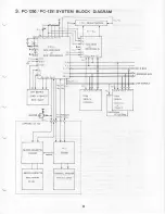
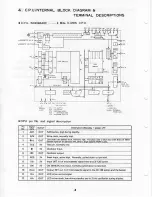
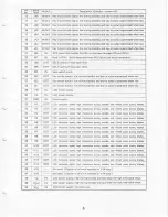

Summary of Contents for PC-1250
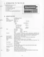
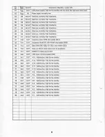
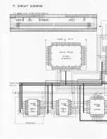
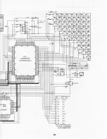
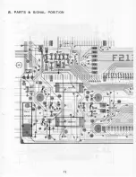
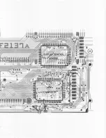
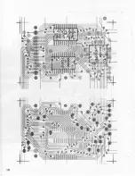
Page 13: ...11 8 PARTS SiGNAL POSiTiON ...
Page 14: ......
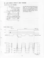
Page 15: ...12 ...
Page 16: ...13 ...
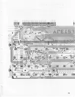
Page 17: ...13 ...
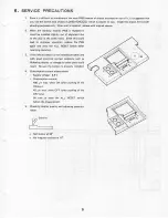
Page 19: ...16 PARTS GUDE ...
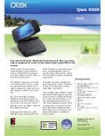
The Sharp PC-1250 is a reliable and efficient handheld computer that assists users with various tasks. To ensure optimal performance, it is essential to have the Service Manual, which can be easily downloaded for free from manualshive.com. This comprehensive manual provides detailed instructions for troubleshooting and maintenance.
Page 13: ...11 8 PARTS SiGNAL POSiTiON ...
Page 14: ......
Page 15: ...12 ...
Page 16: ...13 ...
Page 17: ...13 ...
Page 19: ...16 PARTS GUDE ...