Sharp LQ201U1LW01, Specifications
The Sharp LQ201U1LW01 is a cutting-edge display panel renowned for its exceptional quality. With detailed specifications and a user-friendly interface, this product offers a truly immersive visual experience. To unlock its full potential, download the comprehensive manual for free from manualshive.com and unleash the possibilities of your new Sharp LQ201U1LW01.
Share
Download


Reviews:
No comments
Related manuals for LQ201U1LW01
TY-FB9BD
Brand: Panasonic Pages: 1
DVK-300HD
Brand: Datavideo Pages: 45

HDP 171
Brand: Kathrein Pages: 52
DroidTV C2
Brand: Fantec Pages: 5
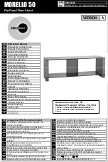
MORELLO50
Brand: Omnimount Pages: 16
DSM-382
Brand: Boxee Pages: 18
DTT9001
Brand: Jiuzhou Pages: 30

Safety Belt A-552
Brand: Da-Lite Pages: 4
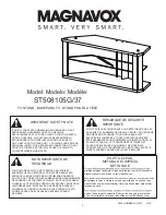
ST508105G/37
Brand: Magnavox Pages: 8

Terrestrial Signal Finder
Brand: Terrestrial Signal Finder Pages: 26

TV PicShare
Brand: Armchair Pages: 48
IWPE2-TV-7FT
Brand: DataComm Electronics Pages: 3

TV Accessories
Brand: Veebeam Pages: 53
EchoLink IR
Brand: Echo Pages: 16
ECO-12
Brand: A2B Electronics Pages: 8
Smart TV Cam
Brand: biscotti Pages: 26
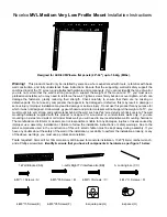
MVL
Brand: Rocelco Pages: 7
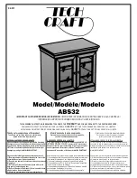
ABS32
Brand: Tech Craft Pages: 8


