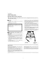
background image


SERVICE MANUAL

Parts marked with "

" are important for maintaining the safety of the set. Be sure to replace these parts with specified ones for maintaining the

safety and performance of the set.

This document has been published to be used for
after sales service only.
The contents are subject to change without notice.

SAFETY PRECAUTION

IMPORTANT SERVICE SAFETY PRE-
CAUTION ............................................................i
PRECAUTIONS A PRENDRE LORS DE 
LA REPARATION ...............................................ii
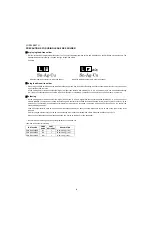
PRECAUTIONS FOR USING LEAD-FREE 
SOLDER ........................................................... iii

OUTLINE

MAJOR SERVICE PARTS ................................iv

CHAPTER 1. SPECIFICATIONS

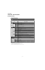
[1] SPECIFICATIONS ......................................... 1-1

CHAPTER 2. OPERATION MANUAL

[1] OPERATION 

MANUAL .................................. 2-1

CHAPTER 3. DIMENSIONS

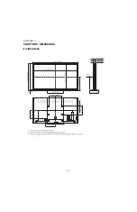
[1] DIMENSIONS ................................................ 3-1

CHAPTER 4. REMOVING OF MAJOR PARTS

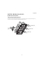
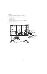
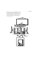
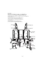
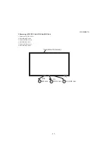
[1]  REMOVING OF MAJOR PARTS ................... 4-1
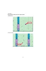
[2]  The location putting on the heat measure 

sheet .............................................................. 4-6

[3]  Precautions for assembly............................... 4-7

CHAPTER 5. ADJUSTMENT

[1] ADJUSTMENT 

PROCEDURE ......................5-1

[2]  PUBLIC MODE SETTING PROCEDURE

......5-17

CHAPTER 6. TROUBLESHOOTING TABLE

[1]  Failure diagnosis by LED in front of cabinet .........6-1
[2]  LED flashing specification at the time of an 

error (Center icon LED used) ........................6-1

[3] TROUBLESHOOTING 

TABLE ......................6-4

CHAPTER 7. MAJOR IC INFORMATIONS

[1] MAJOR 

IC 

INFORMATIONS .........................7-1

CHAPTER 8. OVERALL WIRING/SYSTEM BLOCK 
DIAGRAM

[1]  OVERALL WIRING DIAGRAM......................8-1
[2]  SYSTEM BLOCK DIAGRAM.........................8-2

Parts Guide

TopPage

CONTENTS

LC-90LE657U

LCD COLOR TELEVISION

LC-90LE657U

MODEL

In the interests of user-safety (Required by safety regulations in some countries) the set should be restored to its orig-
inal condition and only parts identical to those specified should be used.

No. S53B6LC90LE65

Summary of Contents for LC-90LE657U

Page 1: ...JOR PARTS 1 REMOVING OF MAJOR PARTS 4 1 2 The location putting on the heat measure sheet 4 6 3 Precautions for assembly 4 7 CHAPTER 5 ADJUSTMENT 1 ADJUSTMENT PROCEDURE 5 1 2 PUBLIC MODE SETTING PROCEDURE 5 17 CHAPTER 6 TROUBLESHOOTING TABLE 1 Failure diagnosis by LED in front of cabinet 6 1 2 LED flashing specification at the time of an error Center icon LED used 6 1 3 TROUBLESHOOTING TABLE 6 4 CH...

Page 2: ... AC voltage drop across the resistor All checks must be repeated with the AC cord plug connection reversed If necessary a nonpolarized adaptor plug must be used only for the purpose of completing these checks Any reading of 0 75 Vrms this corresponds to 0 5 mA rms AC or more is excessive and indicates a potential shock hazard which must be corrected before returning the monitor to the owner SAFETY...

Page 3: ... et de compartiment les réseaux de résistancecapacité les isolateurs mécaniques etc S assurer qu il n y ait pas de danger d électrocution en vérifiant la fuite de courant de la facon suivante Brancher le cordon d alimentation directem ent à une prise de cou rant de 120V Ne pas utiliser de transformateur d isolation pour cet essai A l aide de deux fils à pinces brancher une résistance de 1 5 kΩ 10 ...

Page 4: ... solder by 40 C and as it has poor solder wettability you may be apt to keep the soldering bit in contact with the PWB for extended period of time However Since the land may be peeled off or the maximum heat resistance temperature of parts may be exceeded remove the bit from the PWB as soon as you confirm the steady soldering condition Lead free solder contains more tin and the end of the solderin...

Page 5: ...KG015FM02 R C OPC Unit N RUNTKA936WJQZ WiFi Unit N RUNTKB126WJQZ BLUETOOTH Unit N RUNTKB096WJQZ POWER DRIVER Unit Ref NO PARTS CODE DESCRIPTION N R1LK900D3GW10Z 90 LCD PANEL Unit LK900D3GW10Z Ref No Parts No Description Q ty IC2004 RH iXD515WJN7Q IC Monitor Microprocessor 1 Ref No PARTS CODE DESCRIPTION Q ty N QCNW C222WJQZ Connecting Cord L 1000mm 80pins LCD Control Unit to LCD Panel Unit x2 2 N ...

Page 6: ...LC 90LE657U 1 1 LC 90LE657U Service Manual CHAPTER 1 SPECIFICATIONS 1 SPECIFICATIONS ...

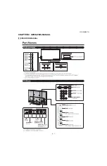
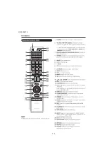
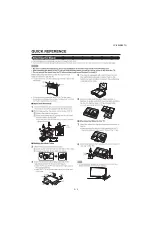
Page 7: ...LC 90LE657U 2 1 LC 90LE657U Service Manual CHAPTER 2 OPERATION MANUAL 1 OPERATION MANUAL ...

Page 8: ...LC 90LE657U 2 2 ...

Page 9: ...LC 90LE657U 2 3 ...

Page 10: ...LC 90LE657U 3 1 LC 90LE657U Service Manual CHAPTER 3 DIMENSIONS 1 DIMENSIONS ...

Page 11: ...move the 4 lock screws 1 and detach the Stand Unit 2 2 Remove the 3 lock screws 3 20 lock screws 4 10 lock screws 5 and detach the Rear Cabinet L Ass y 6 Rear Cabinet R Ass y 7 3 Remove the 5 lock screws 8 8 lock screws 9 and detach the Rear Cabinet C Ass y 10 4 3 4 5 1 2 Stand Unit 6 Rear Cabinet L Ass y 7 Rear Cabinet R Ass y 10 Rear Cabinet C Ass y 9 8 ...

Page 12: ...he RC Wire 4 Detach the KEY Unit Ass y 4 5 Disconnect the KM Wire 6 Remove the 2 lock screws 5 and detach the KEY Button 6 from KEY Button cover 8 7 Detach the KEY Unit 7 from KEY button 6 8 Disconnect the SB Wire 9 Detach the Speaker Woofer 9 7 5 4 8 6 Key Button KEY Unit KEY Unit Ass y Key Button Cover SP KM SP RC MAIN Unit 3 1 Speaker R 2 1 Speaker L 9 Speaker Woofer SB SB ...

Page 13: ...g connectors from the LCD CONTROL Unit PL LV 4 Remove the 16 lock screws 1 and detach the 16 Module Fix Angle Ass y 2 5 Remove the 7 Hooks and detach the 90 LCD Panel Module Unit Ass y 3 6 Remove the 2 Bottom Covers 4 1 2 2 1 1 2 Module Fix Angle Ass y Module Fix Angle Ass y Module Fix Angle Ass y MAIN Unit LCD Control Unit POWER DRIVER Unit Hook Hook L1 L2 PD PD PL LV 3 90 LCD Panel Module Unit A...

Page 14: ...tand Angle Ass y 13 6 Remove the 16 lock screws 14 and detach the 4 VESA Angle Ass y 15 7 Disconnect the BT wire 8 Detach the BLUETOOTH Unit 18 from the Speaker Holder 17 9 Remove the 4 lock screws 16 and detach the 2 Speaker Holder 17 90 LCD Panel Module Unit 11 10 1 FFC Cord LCD CONTROL Unit 12 3 13 12 POWER DRIVER Unit Stand Angle Ass y 13 Stand Angle Ass y 8 5 4 Terminal Angle Bottom Terminal ...

Page 15: ... ICON Unit WiFi Unit 1 Detach the R C OPC Unit 1 2 Disconnect the RA wire 3 Detach the ICON Unit 3 4 Disconnect the CI wire 5 Detach the WiFi Unit 2 6 Disconnect the UB wire Decoration Frame Ass y 3 ICON Unit 2 WiFi Unit 1 R C OPE Unit RA UB CI ...

Page 16: ...LC 90LE657U 4 6 2 The location putting on the heat measure sheet 1 MAIN PWB Unit 2 LCD Control Unit PSPAZC871WJKZ PSPAZC854WJKZ ...

Page 17: ...hat the EMI prevention parts are not peeled and twisted from the access holes The EMI prevention parts conductive nonwoven fabric gaskets must be seen from the access holes Countermeasure Attach the conductive nonwoven fabric gaskets on the shielded case on the main PWB PMLT A678WJQZ Attach the conductive nonwoven fabric gasket on the RF terminal angle PMLT A680WJQZ ...

Page 18: ...wing is a drawing mounting the main PWB Ass y on the backlight chassis The parts indicated by are the access holes for confirmation Main PWB Ass y State where the shielded case and RF terminal angle are mounted on the main PWB ...

Page 19: ...lease use a software version after OKLAMxxx SMB The main software monitor microprocessor software can be upgraded by using a general purpose USB Memory The followings are the procedures for upgrading explained separately for the main software monitor microprocessor software 2 2 Main software version upgrade 2 2 1 Get ready before you start USB Memory of 128MB or higher capacity PC running on Windo...

Page 20: ...nformation appears after the upgrade is complete 8 Unplug the AC cord and remove the USB Memory for version upgrade 9 Now the software version upgrade is complete NOTE When you are done with the software version upgrade start the set go to the top page of the adjustment process screen and check the main software version information MAIN SUB MICOM PANEL EEPROM MAIN Version SUB MICOM Version PANEL E...

Page 21: ...minor upgrade 6 If the upgrade fails power led will stop blinking Also the upgrade failure screen will be shown if upgrade screen was shown at 5 NOTE In the event of a transient failure upgrade will be automatically retried up to three times If the process repeatedly fails hardware may be the cause 7 The upgrade success screen will be shown if upgrade screen was shown at 5 8 Unplug the AC cord and...

Page 22: ... mode If the settings are tampered in this mode unrecoverable system damage may result 4 Remote controller key operation and description of display in adjustment process mode 1 Key operation Input mode is switched automatically when relevant adjustment is started so far as the necessary input signal is available 2 Description of display Remote controller key Main unit key Function CH CH Moving an ...

Page 23: ...D 10 VIC YPOS Y coordinate setting for VIC READ 11 VIC COLOR Collected color data setting for VIC READ 12 VIC SIGNAL TYPE Signal type setting for VIC READ 13 VIC READ Picture level acquisition function Level appears in green on the upper right 3 1 N358 ALL ADJ INPUT2 CVBS and TUNER signal level adjustment 2 N358 MAIN ADJ INPUT2 CVBS signal level adjustment 3 TUNER DAC ADJ TUNER signal level adjust...

Page 24: ... 3 R adjustment value 10 MG3G WB adjustment Point 3 G adjustment value 11 MG3B WB adjustment Point 3 B adjustment value 12 MG3Y WB adjustment Point 3 Y adjustment value Quattron panel Only 11 1 MG4R WB adjustment Point 4 R adjustment value Parameter for six point adjustment 2 MG4G WB adjustment Point 4 G adjustment value 3 MG4B WB adjustment Point 4 B adjustment value 4 MG4Y WB adjustment Point 4 ...

Page 25: ... 7 CD MID6 8 CD MAX 16 1 CALC 2 RESET 3 VAL1 4 VAL2 5 VAL3 6 VAL4 7 VAL5 8 VAL6 9 GAMMA ADJ TEMP 17 1 MONITOR TIME OUT 2 MONITOR MAX TEMP 3 MONITOR ERROR CAUSE RESET 18 1 LCD TEST PATTERN 2 LCD TEST PATTERN1 3 LCD TEST PATTERN2 4 LCD TEST PATTERN3 5 LCD TEST PATTERN4 6 TV TEST PATTERN 1 7 TV TEST PATTERN 2 19 1 T CON VERSION EXT 1 2 T CON VERSION EXT 2 3 T CON VERSION EXT 3 4 T CON VERSION EXT 4 2...

Page 26: ...TRENGTH 4 INPUT KEY STRENGTH 5 CH UP KEY STRENGTH 6 CH DOWN KEY STRENGTH 7 VOL UP KEY STRENGTH 8 VOL DOWN KEY STRENGTH 25 1 CROSSTALK ADJ MODE 2 CROSSTALK TH1 3 CROSSTALK TH2 4 CROSSTALK TH3 5 CROSSTALK TH4 6 CROSSTALK GAIN1 7 CROSSTALK GAIN2 8 CROSSTALK GAIN3 26 1 WIFI SSID 2 4GHz Set AP SSID 2 WIFI SSID 5GHz Set AP SSID 3 WIFI RSSI 2 4GHz Set RSSI threshold 4 WIFI RSSI 5GHz Set RSSI threshold 5 ...

Page 27: ...ing setting values from EEPROM 3 MODEL NAME 4 PANEL SIZE 5 SETTING FOR ADJ 6 VERUP FLAG ENABLE 7 SHARP RC ENABLE 8 PANEL LIMIT 9 PANEL RANGE LIMIT 10 SHORT CHECK MODE 11 SHORT CHECK CURRENT 12 CURRENT SW 13 TEST NETWORK UPDATE Page Line Item Description Remarks adjustment detail etc ...

Page 28: ...S T CON FPGA status error 54 E_TCON_E T CON hung up Monitor ERR STBY table Outline Communication Power failure detected by the monitor microprocessor is stored in EEPROM and last 4 abnormal can be confirmed in the Process mode A Location Page 1 of the process mode A MONITOR ERR CAUSE 0 if there is no error It is cleared to 0 on the last page of the process mode A Display Error description 02 Initi...

Page 29: ...ng the checker connect the USB memory to the J9502 TL9524 9527 3 Apply the specified voltage to the PWB and boot it up with the tool connected 4 Send the software writing start command via RS232C 5 Send the writing status check command and confirm the response of OK Then turn off the power CAUTION When the USB memory is not inserted or reading error occurs nothing is written Adjustment item Adjust...

Page 30: ...justment remote control Adjustment point Adjustment conditions Adjustment procedure 1 Setting N358 signal US 10ch Send the N358 color bar color saturation 75 signal to the composite input Send the in house signal use US 10ch to TUNER 2 Automatic adjustment exe cution Point the cursor to N358 ALL ADJ INPUT2 and press the Enter key The adjustment is complete when N358 ALL ADJ INPUT2 OK is displayed ...

Page 31: ...J and press the Enter key The adjustment is complete when ANALOG RGB ADJ OK is displayed Adjustment point Adjustment conditions Adjustment procedure 1 Setting NTSC RF signal US 7 AIR ch Send the NTSC signal to the RF antenna input 2 Automatic adjustment exe cution Point the cursor to VCHIP TEST 07ch and press the Enter key Adjust the selected channel to the in house signal The adjustment is OK whe...

Page 32: ...dard value 5 Set the point 3 to the specified gradation set the G correction value 448 x G value of point 6 928 fractions rounded off and adjust the RB so that it becomes the standard value 6 Set the point 2 to the specified gradation set the G correction value 296 x G value of point 6 928 fractions rounded off and adjust the RB so that it becomes the standard value 7 Set the point 1 to the specif...

Page 33: ...tting CAUTION Do not turn on the power after completing the factory setting If the power is turned on configure the factory setting again Adjstment point Adustment conditions Adjstment procedure 1 HDMI EDID writing Analog RGB EDID writing Main PWB Process mode Model discrimination check 1 Enter the process mode 2 Point the cursor to HDMI EDID WRITE and press the ENT key The writing is complete whe...

Page 34: ...3 T CON ROM PRIMROSE_CMB G281 _2013022842667701_485BCD3 ROM 13 Writing the inch and model name onto EEPROM 1 Enter the adjustment process mode 2 Point the cursor to MODEL NAME Page 29 29 3 Select LE657U and press Enter key 4 OK is displayed 5 Point the cursor to PANEL SIZE Page 29 29 6 Select 90 and press Enter key 7 Moments later image is displayed 8 Turn off power 9 Turn on power ...

Page 35: ... to exit Public Mode There are the following ways to quit the public mode setup screen Turn off PUBLIC MODE in the adjustment process mode This way alone is not for quitting the setup screen but for quitting the mode itself Turn off the power with the POWER key Select EXECUTE PUBLIC MODE stays on in the adjustment process mode The settings will be back to the factory ones 3 Public Mode Setting Val...

Page 36: ...nd VOL key remote controller and set To save new settings keep the cursor at EXECUTE and use ENTER key remote controller and set PUBLIC MODE POWER ON FIXED VARIABLE MAXIMUM VOLUME 60 VOLUME FIXED VARIABLE VOLUME FIXED LEVEL 20 RC BUTTON RESPOND PANEL BUTTON RESPOND MENU BUTTON RESPOND AV POSITION FIXED VARIABLE ON SCREEN DISPLAY YES INPUT MODE START NORMAL INPUT MODE FIXED VARIABLE LOUD SPEAKER ON...

Page 37: ...he INPUT and Vol keys which are on the tact key 3 Enter the passward by using R C The passward is 027 4 Select COPY MODE 5 The follow guide is displayed Then select the TV USB Start 6 Follow guide is displayed when it is finished then select Reset TV will restart 7 Insert the USB which has the data from TV to another TV or itself 8 Insert AC code of the TV with pushing the INPUT and Vol keys which...

Page 38: ...LC 90LE657U 5 20 10 The following guide is dispalyed Then select the USB TV Start 11 Follow guide is displayed when it is finished then select Reset TV will restart 12 Comfirm the user setting is copied ...

Page 39: ...ecified for a fixed volume at start Limit in Setting The sound volume for the ON timer Wake up timer is fixed also without display of menu Besides the setting is made impossible Basically the menu is not displayed The following keys become invalid Sound volume Up Down VOL for both remote control and the unit Mute MUTE Exception In the item VOLUME of adjustment process the sound volume can be set f...

Page 40: ...layed This is because the channel call message may be confused with a message being sent from the hotel On the North America destined models the OSD works the same as at the No setting Limit in Setting Keys falling under any of the following items become invalid Appearance of screen changes and the sound changes Personal functions which are hard to restore Screen display menu OFF timer ON timer AV...

Page 41: ...ection between OFF ON TV RCE and ON TV RCD loop provided Default OFF Explanation Function to feed the remote controller received signal to Pin 9 open on the RS232C Limit in Setting None Exception None Remarks None Selection Selection between Variable and Fixed loop provided Default Variable Explanation In case of Fixed setting Menu Picture and Audio setting can t be changed like Dynamic Fixed When...

Page 42: ...Selection Selection between ON and OFF loop provided Default OFF Explanation In case of ON public mode settings are effected Limit in Setting None Exception None Remarks The public mode settings are operable only when this item is set at ON ...

Page 43: ... once Lamp error Power PWB failure Power failure etc Flashes twice Flash once Power supply error 2 2 AC_DET error Flash twice Power supply error 2 2 UR 13V error Flash 3 times Power supply error 2 2 D 3 3V error Flash 5 times Panel power supply error Main PWB failure Communication failure etc Flashes 3 times Flashes once Initial communication error Flashes twice Start up confirmation communication...

Page 44: ... cannot be activated except in the adjustment process mode Accumulated counts are cleared to 0 by the setting in the LAMP ERROR RESET on the adjustment process mode Error type Center icon LED operation Pins are monitor microcomputer pins unless other wise specified PS_ON AC_DET failure Flashes fast once H On L Off AC_DET failure L SM_POW Main 13V failure Flashes fast twice H On L Off DET_13V failu...

Page 45: ...on failure Flashes fast 3 times H On L Off Regular communication that is performed at 1 second intervals in the normal operation is interrupted Main CPU operation failure or monitor microcom puter reception failure Other communica tion failure Flashes fast 5 times H On L Off When a request PM_REQ H is sent from the main microcomputer the request command is not output from the main CPU etc Main CPU...

Page 46: ...ars in the panel module When the parts in the panel cannot be replaced Replace panel module If it is not an error of power supply LED driver It is start up in the lamp error disregard mode Do you start NO When power supply unit is replaced does it start normally YES NO Replace power supply unit When main unit is replaced does it start normally YES NO Replace main unit When LCD control unit is repl...

Page 47: ...hen C S FPC is replaced does screen display normally NO YES Replace C S FPC When C PWB is replaced does screen display normally NO YES Replace C PWB Adjust VCOM ADJ after replace C PWB Replace Panel HIRAKI Adjust VCOM ADJ after replace Panel HIRAKI ...

Page 48: ...e adjustment process mode and display LCD TEST PATTERN of 18 page Please press volume keys and a test pattern is displayed Is it all usually displayed YES It isn t the fault of a C PWB Please check operation with reference to other items NO Is only the half of the right screen or the left screen displayed normally YES It is checked whether FFC to Panel is connected correctly Replace another C PWB ...

Page 49: ...signal at input pins of IC3301 CPU NO Check the TMDS line between SC1501 and IC2601 and its peripheral circuits IC2601 TMDS input pins pin 26 27 CLK pin 28 29 D0 pin 30 31 D1 pin 31 33 D2 YES Check the TMDS line between IC2601 and IC3301 and its peripheral circuits IC3301 TMDS input pins pin AH35 AH34 CLK pin AG35 AG34 D0 pin AG37 AG36 D1 pin AF35 AF34 D2 Check the I2C line between IC2601 and IC33...

Page 50: ... signals at input pin of IC3301 CPU NO Check the TMDS line between SC1502 and IC2601 and its peripheral circuits IC2601 TMDS input pins pin 17 18 CLK pin 19 20 D0 pin 21 22 D1 pin 23 24 D2 YES Check the TMDS line between IC2601 and IC3301 and its peripheral circuits IC3301 TMDS input pins pin AH35 AH34 CLK pin AG35 AG34 D0 pin AG37 AG36 D1 pin AF35 AF34 D2 Check the I2C line between IC2601 and IC3...

Page 51: ... signal at input pins of IC3301 CPU NO Check the TMDS line between SC1503 and IC2601 and its peripheral circuits IC2601 TMDS input pins pin 8 9 CLK pin 10 11 D0 pin 12 13 D1 pin 14 15 D2 YES Check the TMDS line between IC2601 and IC3301 and its peripheral circuits IC3301 TMDS input pins pin AH35 AH34 CLK pin AG35 AG34 D0 pin AG37 AG36 D1 pin AF35 AF34 D2 Check the I2C line between IC2601 and IC330...

Page 52: ...TMDS signal at input pins of IC3301 CPU NO Check the TMDS line between SC1504 and IC2601 and its peripheral circuits IC2601 TMDS input pins pin 99 100 CLK pin 1 2 D0 pin 3 4 D1 pin 5 6 D2 YES Check the TMDS line between IC2601 and IC3301 and its peripheral circuits IC3301 TMDS input pins pin AH35 AH34 CLK pin AG35 AG34 D0 pin AG37 AG36 D1 pin AF35 AF34 D2 Check the I2C line between IC2601 and IC33...

Page 53: ... AU26 AP25 Y AR26 Pb and AP26 Pr of IC3301 CPU YES NO Check the line between the input terminals of J510 and IC3301 J510 pin 18 Y pin 16 Pb pin 15 Pr IC3301 pin AU26 AP25 pin AR26 pin AP26 Is the T CON PWB connected VBO_HTPDN pin 40 of SC3801 become Low if there is no problem in the connection NO Check the T CON PWB and harness Check IC3301 and SC3801 and their periph eral circuits in Main PWB YES...

Page 54: ...10 and pin E28 of IC3301 CPU J510 pin 4 IC3301 pin E28 Is there the COMPOSITE signal input at pin AR31 of IC3301 CPU Is there the COMPOSITE signal input at pin AR30 of IC3301 CPU YES NO YES NO Check the line between pin 10 of J510 and pin AR31 of IC3301 CPU J510 pin 10 IC3301 pin AR31 Check the line between pin 5 of J510 and pin AR30 of IC3301 CPU J510 pin 9 IC3301 pin AR30 Is the T CON PWB connec...

Page 55: ... R of IC3301 CPU Are there the VSYNC HSYNC signal inputs at pins AM25 and AN25 of IC3301 YES NO Check the line between SC510 and IC3301 and their peripheral circuits Is the T CON PWB connected VBO_LOCKN pin 40 of SC3801 become Low if there is no problem in the connection NO Check the T CON PWB and harness Check IC3301 and SC3801 and their peripheral circuits in Main PWB YES Are the V By One HS sig...

Page 56: ...4 and their peripheral circuits Check the Tuner I2C lines TU1104 pin 5 TUN_SCL pin 4 TUN_SDA IC3301 pin V35 pin V34 Check the IF AGC line between pin U35 of IC3301 and pin 12 of TU1104 Check the Tuner I2C lines TU1104 pin 5 TUN_SCL pin 4 TUN_SDA IC3301 pin V35 pin V34 Is the T CON PWB connected VBO_LOCKN 40pin of SC3801 become Low if there is no problem in the connec tion NO Check the T CON PWB an...

Page 57: ...peripheral circuits IC1508 IC1509 etc YES Are there the TMDS signal at input pin 1 2 D0 of IC2601 HDMI SW NO Check the TMDS line between SC1504 and IC2601 and its peripheral circuits IC1504 etc YES Are there the TMDS signal at input pins of IC3301 CPU NO Check the TMDS line between IC2601 and IC3301 and its peripheral circuits IC3301 TMDS input pins pin AH35 AH34 CLK pin AG35 AG34 D0 pin AG37 AG36...

Page 58: ...d AT35 R of IC3301 CPU YES NO YES NO YES NO Check the line between J510 and IC3301 Check the line between J510 and IC3301 Check the line between J510 and IC3301 Does the digital audio signal come from pins AR11 AP11 AN9 CPU_AOBCK AOLRCK AOSDATA0 of IC3301 CPU to pins 6 7 5 SP_BCLK SP_LRCLK SP_DATA of IC1703 Audio DSP YES NO Check the line between IC3301 and IC1703 and their paripheral circuits Abo...

Page 59: ...pins AR11 AP11 AN9 CPU_AOBCK AOLRCK AOSDATA0 of IC3301 CPU to pins 6 7 5 SP_BCLK SP_LRCLK SP_DATA of IC1703 Audio DSP YES NO Check the line between IC3301 and IC1703 and their peripheral circuits About the L R Speakers Does the digital audio signal come from pins 30 21 26 27 of IC1703 Audio DSP to pin 5 7 8 6 of IC1902 AMP for L R About the Subwoofer speaker Does the digital audio signal come from...

Page 60: ... DSP YES NO Check the line between IC3301 and IC1703 and their paripheral circuits About the L R Speakers Does the digital audio signal come from pins 30 21 26 27 of IC1703 Audio DSP to pin 5 7 8 6 of IC1902 AMP for L R About the Subwoofer speaker Does the digital audio signal come from pins 30 21 26 28 of IC1703 Audio DSP to pin 5 7 8 6 of IC1901 AMP for SW YES NO Check IC1703 and its paripheral ...

Page 61: ...O Set the audio output to FIXED Does the digital audio signal come from pins AR11 AP11 AN9 CPU_AOBCK AOLRCK AOSDATA0 of IC3301 CPU to pins 6 7 5 SP_BCLK SP_LRCLK SP_DATA of IC1703 Audio DSP YES NO Check the line between IC3301 and IC1703 and their peripheral circuits About the L R Speakers Does the digital audio signal come from pins 30 21 26 27 of IC1703 Audio DSP to pin 5 7 8 6 of IC1902 AMP for...

Page 62: ... and its peripheral circuits Is there the SPDIF signal OPT_OUT input at pin 2 of IC503 SPDIF BUFFER SPDIF MUTE YES NO Check the line between IC3301 and IC503 Is there the MUTE signal input at pin 1 of IC503 usual High Mute Low YES NO Check the AUDIO_MUTE and their peripheral circuits Q505 etc Is there the SPDIF signal input at pin 1 of D527 OPTICAL OUTPUT YES NO Check the speakers and the optical ...

Page 63: ... pins 3 L and 2 R of J504 YES NO Check the line between IC1702 and J504 and their peripheral circuits Check the LINE_MUTE line and its peripheral circuits Q506 Q510 etc Check the connector J504 and their peripheral circuits and speakers and the Cable No connect network Does the signal come to 1pin of LAN jack J9401 see fig 1 fig 2 NO Check the interface device and peripheral circuits power LED of ...

Page 64: ...udio decoder a four link LVDS transmitter a V by One transmitter and an NTSC PAL SECAM TV decoder with a 3D comb filter NTSC PAL It supports Full HD MPEG1 2 4 H 264 DiviX VC1 RM AVS VP6 VP8 video decoder standards and JPEG Audio support includes a BTSC and a Dolby AC3 MPEG 2 Layer 1 2 audio decoder Two SPDIF output and a pair of analog outputs L R are provided The LSI incorporates a complete ARM C...

Page 65: ...iAK4201EU 1Y This IC is audio amplifier for line out head phone 1 12 IC1703 VHiYSS952QZ 1Y Audio DSP YSS952QZ has digital audio adjustment function for example PEQ bass treble balance bass enhancer etc and adjusts TVs audio quality ...

Page 66: ...LC 90LE657U 7 3 MEMO ...

Page 67: ...䇽 㪧㪦㪮㪜㪩㪆㪛㪩㪠㪭㪜㪩 㪩㪬㪥㪫㪢㪙㪇㪐㪍㪮㪡㪨㪱 㪨㪘㪚㪚㪛㪘㪇㪐㪌㪮㪡㪧㪱 㪨㪚㪥㪮㪄㪤㪊㪍㪈㪮㪡㪨㪱 㪨㪚㪥㪮㪄㪥㪋㪋㪋㪮㪡㪱㪱 㪨㪚㪥㪮㪄㪤㪏㪌㪏㪮㪡㪧㪱 㪨㪚㪥㪮㪄㪤㪎㪎㪎㪮㪡㪨㪱 㪨㪚㪥㪮㪄㪥㪉㪌㪋㪮㪡㪱㪱 㪨㪚㪥㪮㪄 㪤㪎㪎㪍㪮㪡㪨㪱 㪨㪚㪥㪮㪄 㪤㪎㪎㪋 㪮㪡㪨㪱 㪨㪚㪥㪮㪄㪥㪋㪋㪊㪮㪡㪱㪱 㪋 㪈 䇼㪧㪣䇽 䇼㪘㪚䇽 㪉㪋 㩷㩷㪈 㪣㪚㪛㩷㪚㪦㪥㪫㪩㪦㪣 㪛㪬㪥㪫㪢㪞㪉㪏㪈䌆䌍㪇㪉 䇼㪢㪤䇽 㩷㩷㩷㩷㪢㪜㪰 㪛㪬㪥㪫㪢㪝㪏㪇㪇㪝㪤㪌㪊 䇼㪠㪩䇽 䇼㪙㪫䇽 㪈 㪉㪋 䇼㪧㪛䇽 䇼㪬㪙䇽 㪈 㪍 䇼㪬㪙㩷䇽 㪈㩷㩷㩷㩷㪍 㪮㫀㪝㫀 㪩㪬㪥㪫㪢㪘㪐㪊㪍㪮㪡㪨㪱 䇼㪩㪘䇽 㪈㩷㩷㩷㩷㪌 㪩㪆㪚㩷㪦㪧㪚 㪛㪬㪥㪫㪢㪞㪇㪈㪌㪝㪤㪇㪉 㪬㪪㪙 㪜㪫㪟㪜㪩 㪥㪜㪫 㪣㪺㪿䋺㪩㪪㪧㪄㪱㪘㪌㪊㪏㪮㪡㪨㪱 㪈 㩷㩷㩷㩷㩷㩷㩷㩷㩷㩷㪋 䇼㪣㪭䇽 㪈 㪋㪈 㪈㪌㵘 㪈 䇼㪣㪈䇽 㪬㪪㪙 㪟㪛...

Page 68: ...LC 90LE657U 8 2 2 SYSTEM BLOCK DIAGRAM 1 2 3 10 9 7 6 5 4 8 J A B C D E F G H I 13 11 19 18 16 15 14 12 17 ...

Page 69: ...f the set This document has been published to be used for after sales service only The contents are subject to change without notice LC 90LE657U PartsGuide 1 PRINTED WIRING BOARD ASSEMBLIES 2 LCD PANEL MODULE UNIT 3 CABINET AND MECHANICAL PARTS 4 SUPPLIED ACCESSORIES PACKING PARTS 5 SERVICE JIG USE FOR SERVICING CONTENTS LCD COLOR TELEVISION LC 90LE657U MODEL No S53B6LC90LE65 ...

Page 70: ... MAIN Unit N DUNTKG281FM02 BN X LCD CONTROL Unit N DUNTKG014FM02 AF X ICON Unit N DUNTKG015FM02 AF X R C OPC Unit N DUNTKF800FM53 AE X KEY Unit N RUNTKA936WJQZ AX X WiFi Unit N RUNTKB126WJQZ AT N X BLUETOOTH Unit N RUNTKB096WJQZ BR N X POWER DRIVER Unit 2 LCD PANEL MODULE UNIT N R1LK900D3GW10Z HZ N X 90 LCD PANEL Unit LK900D3GW10Z ...

Page 71: ...7 2 D 7 3 7 3 7 3 15 27 21 19 PL LV FF H LCD CONTROL Unit 24 10 18 20 15 PD G MAIN Unit SP UB LV BT SB 5 6 5 15 5 15 5 8 5 8 5 1 5 1 5 1 5 1 5 4 5 2 5 5 5 15 5 8 5 15 5 9 5 15 5 15 5 15 5 15 5 5 13 5 7 34 5 11 UB WiFi Unit 5 12 KM RA CI RC CI ICON Unit RA R C OPC Unit 5 14 5 3 16 16 29 22 28 31 31 14 14 SP 33 36 41 37 40 39 4 6 4 1 4 5 4 5 4 5 4 3 4 4 4 2 3 4 4 3 3 3 3 3 3 3 3 3 1 3 2 3 2 2 2 2 2 ...

Page 72: ... XBPS830P08000 AA J Screw x23 6 CANGKD398WJ31 AF X VESA Angle Ass y x4 6 1 Not Available N VESA Angle 6 2 Not Available N VESA Shaft 7 CANGKD639WJ31 AM N X Stand Angle Ass y x2 7 1 Not Available N Stand Angle 7 2 LHLDWA133WJKZ AC J Wire Holder 7 3 Not Available Himeron x4 8 GCOVAE164WJ3A AX J Bottom Cover x2 9 LANGKD145WJFW AD X Terminal Angle Side 10 LANGKD292WJ3W AD X Terminal Angle Bottom 11 LH...

Page 73: ... S7 S7 S7 S8 S8 S8 S9 S9 S3 S10 S5 S1 S6 S2 S4 S12 X4 X9 X6 X12 X5 X11 X1 X3 X2 Stand Base Ass y Support Ass y Stand Screw Ass y X7 X8 Enquete Card Remote control unit AAA size battery Stand unit 3D Glasses AC cord AA Live Card Operation Manual 3D Glasses X10 3D Glasses Manual Connection Guide ...

Page 74: ...n NOT REPLACEMENT ITEM S3 SPAKFC204WJZZ N Front Pad Base NOT REPLACEMENT ITEM S4 SPAKLA006WJZZ N Joint x5 NOT REPLACEMENT ITEM S5 SPAKPB869WJZZ N Polyethylene Bag NOT REPLACEMENT ITEM S6 SPAKWA005WJZZ N Pallet NOT REPLACEMENT ITEM S7 SPAKXD673WJZZ N Packing Form Top NOT REPLACEMENT ITEM S8 SPAKXD674WJZZ N Packing Form Bottom NOT REPLACEMENT ITEM S9 SPAKXD675WJZZ N Packing Form Side NOT REPLACEMENT...

Page 75: ...LC 90LE657U ...

Page 76: ...produced stored in a retrieval system or transmitted in any from or by any means electronic mechanical photocopying recording or otherwise without prior written permission of the publisher SHARP CORPORATION Digital Information Appliance Group CS Promotion Center Yaita Tochigi 329 2193 Japan May 2013 YK DS ...

Page 77: ...been published to be used for after sales service only The contents are subject to change without notice OUTLINE OUTLINE i CHAPTER 1 PRINTED WIRING BOARD ASSEM BLIES 1 MAIN Unit 1 1 2 LCD CONTROL Unit 1 5 CHAPTER 2 SCHEMATIC DIAGRAM 1 DESCRIPTION OF SCHEMATIC DIAGRAM 2 1 2 SCHEMATIC DIAGRAM 2 2 Parts Guide TopPage LC 90LE657U CONTENTS No S53B6LC90LE6P LCD COLOR TELEVISION LC 90LE657U MODEL PWB Uni...

Page 78: ...57U Service Manual OUTLINE OUTLINE We inform you that service parts in the PWB Unit NOTE Replace MAIN Unit DKEYMF953FM06 in case of IC3103 failure Unit Name Description DKEYMF953FM06 MAIN Unit DUNTKG281FM02 LCD CONTROL Unit ...

Page 79: ...LC 90LE657U 1 1 LC 90LE657U Service Manual CHAPTER 1 PRINTED WIRING BOARD ASSEMBLIES 1 MAIN Unit 1 2 3 10 9 7 6 5 4 8 J A B C D E F G H I 13 11 19 18 16 15 14 12 17 MAIN Unit Side A ...

Page 80: ...520 R 1774 C3101 R 2521 R 1969 Q509 R 2522 C3102 R 1776 R 2523 C3103 R1777 R 2524 C3104 R1778 R 2525 R 2526 R 2527 R2528 Q511 L2601 R2529 R 1971 Q512 L2602 Q513 L2603 Q514 L502 R2530 L504 R2531 R2532 C3112 R2533 R2534 R2535 R2536 R 2537 R2538 R 2539 R 2540 FL501 FL502 FL503 R2544 D3101 D3102 D3103 FL508 FL509 R 3102 R3103 IC3101 IC3102 D3302 IC3103 D3304 IC3104 D3305 VA501 F L516 D3306 VA502 F L51...

Page 81: ...LC 90LE657U 1 3 1 2 3 10 9 7 6 5 4 8 J A B C D E F G H I 13 11 19 18 16 15 14 12 17 MAIN Unit Side B ...

Page 82: ...9 R3111 C3521 C3522 R 3306 R3112 R 3113 C3523 R3307 R 3308 C3330 C3524 R3114 VA508 R 3309 R3115 C3525 C3331 VA509 R 3116 C3526 C3332 IC3302 IC3303 C3333 C3527 R3118 C3334 D3310 C3528 C3335 C3529 D3311 D3312 R 3502 C3336 C1202 R 3503 C3337 D3313 C1203 C3338 R3310 C1204 VA510 R 3311 C3339 R3505 VA511 C1205 C1206 R3506 R3312 VA512 C1207 R 3313 R3507 VA513 C1208 D3318 R 3314 C3530 VA514 D3319 R 3121 C...

Page 83: ...LC 90LE657U 1 5 2 LCD CONTROL Unit 1 2 3 10 9 7 6 5 4 8 J A B C D E F G H I 13 11 19 18 16 15 14 12 17 LCD CONTROL Unit Side A ...

Page 84: ... R5851 C6819 R 6215 R5852 C6240 R6218 IC6210 C6241 IC6212 C6242 R5856 C6243 C6820 C6244 R5859 C6245 C6821 C6822 C6246 C6247 C6248 C6825 C6826 R5860 R6801 R6802 R 6226 R5862 R 6227 R5863 R 6228 C6250 R5865 R6229 C6252 R 5672 R 5673 C6253 C6254 R5868 R 5674 R5869 R 5675 R 6809 C6255 C6256 IC6802 C6257 R 5677 C6258 R 6230 R 5678 R6231 C6259 C6835 R 5679 R 6232 R 6234 R5871 C6839 R6235 R5872 R6236 R62...

Page 85: ...LC 90LE657U 1 7 1 2 3 10 9 7 6 5 4 8 J A B C D E F G H I 13 11 19 18 16 15 14 12 17 LCD CONTROL Unit Side B ...

Page 86: ...28 R5829 R 4889 R 5830 R 4892 R5833 R4895 R 5835 R4896 R 5642 R 5836 R4897 R 5643 R 5837 R 4898 R 5644 D6201 R 5645 C6802 R 5646 D6202 R 5647 D6203 D6204 R 5648 R 5649 C6809 R 6207 R 5650 R 5651 R5652 C6811 IC6206 C6236 C6813 R 6210 D6214 IC6209 C6816 R5850 C6818 R 6216 R 6217 R 5853 R5660 R 5854 R6219 R5661 IC6211 R 5855 R 5662 R 5857 R 5663 R 5858 R 5664 R 5665 R5666 R5667 C6823 R6220 R5668 C682...

Page 87: ...µF unless otherwise noted P pF µµF 2 All capacitors are 50V unless otherwise noted CAUTION This circuit diagram is original one therefore there may be a slight difference from yours SAFETY NOTES 1 DISCONNECT THE AC PLUG FROM THE AC OUTLET BEFORE REPLACING PARTS 2 SEMICONDUCTOR HEAT SINKS SHOULD BE REGARDED AS POTENTIAL SHOCK HAZARDS WHEN THE CHASSIS IS OPERATING IMPORTANT SAFETY NOTICE PARTS MARKE...

Page 88: ... 5 V out S CL 2_TUNE R 004 D 3 3V 010 T UN_IFP 004 R 1101 1K C 1108 10P R 1151 10K S DA2_TUNE R 004 N_T UN_R ST 004 C PU_IF_AG C 004 C 1123 0 047u C1127 10u 16V K ZA510WJ PZ C1110 0 01u 25V C1195 4 7u 10V K ZA761WJ QZ R 1149 0 C 1109 0 047u 10V C1185 0 01u 25V C 1129 10u 16V K ZA510WJ PZ R 1104 10K M 2 3V 010 TU1104 AA083WJ QZ 1 2 3 4 5 6 7 8 9 10 11 12 FB1105 0241TA FB1106 0241TA FB1109 0241TA FB...

Page 89: ...pe 1 DCD 2 R xD 3 T xD 4 5 6 DSR 7 R TS 8 C TS 9 10 11 C507 1000P R 588 1K R 534 1K D515 E XA697WJ QZ 5 6V F B509 0104TA FB516 0104TA V A522 V XA236WJ R 519 1K R 570 100 R 604 100K F B525 0241TA VA528 V XA236WJ R 578 18 HP_PL UG 004 R 690 0 R 671 1K M3221EIP 1 E N 2 C 1 3 V 4 C 1 5 C 2 6 C 2 7 V 8 R 1_in 9 R 1_out 10 NC 11 T 1_in 12 FO RC EO N 13 T 1_out 14 G ND 15 V cc 16 S HDN R 525 100K R 512 1...

Page 90: ...WR 5V V GA 66 C EC _A 67 INT 68 R E S E T _N 69 G PIO_MC ON 70 C SDA 71 C SC L 72 DSDA3 73 DSC L3 74 C BUS_HP D3 75 R 3P WR 5V 76 T PW R_ CI2C A 77 R SV DL 78 R SV DL 79 T VD D12 80 T X2P 81 T X2N 82 T X1P 83 T X1N 84 T X0P 85 T X0N 86 T XC P 87 T XC N 88 V D D 12 89 V D D 33 90 R 0X CN 91 R 0X CP 92 R 0X 0N 93 R 0X 0P 94 R 0X 1N 95 R 0X 1P 96 R 0X 2N 97 R 0X 2P 98 A VD D12 99 R 1X CN 100 R 1X CP ...

Page 91: ...QZ 4 7u C3302 10V 0 1u C3301 T L3301 G ND_A 0 01u C 3315 F 330 R 3302 0 01u C3314 F 330 R 3301 A192WJ F B3301 10V K ZA761WJ QZ 4 7u C3336 3411A33N 1 Vin G ND 2 3 O N NC 4 Vout 5 G ND_A A192WJ F B3302 10V 0 1u C3351 10V K ZA761WJ QZ 4 7u C3349 10V 0 1u C3346 10 R 3314 10V K ZA761WJ QZ 4 7u C3348 C3339 0 1u C3343 0 1u C3340 0 1u C3344 0 1u C3341 0 1u C3342 0 1u 0 1u C3338 G ND_A K ZA761WJ QZ 4 7u C3...

Page 92: ... RE S E T T 3 A13 NC T 7 A14 NC T 8 A8 T 9 V SS R 9 V DD P 9 V SS N9 V DD M9 V SS L 9 NC K 9 C KE J 9 NC H9 VDDQ G 9 VS S Q F 9 VS S Q E 9 VDDQ D9 V DD C 9 VDDQ B 9 VS S Q A9 V SS A8 V DDQ A7 DQU4 A3 DQU7 A2 DQU5 B 2 V DD C 2 DQU3 D2 VDDQ E 2 VS S Q F 2 DQL 2 G 2 DQL 6 H2 VDDQ J 2 V SS K 2 V DD L 2 CS M2 B A0 N2 A3 P 2 A5 R 2 A7 R 3 A9 R 7 A11 R 8 A6 P 8 A4 N8 B A1 M8 V RE FC A L 8 ZQ K 8 V DD J 8...

Page 93: ... C 3106 0 1u R 3101 4 7K NAND_D1 004 NAND_D3 004 IXD584WJ QZ F LASH 2Gbit 1 NC 2 NC 3 NC 4 NC 5 NC 6 NC 7 R B 8 R E 9 C E 10 NC 11 NC 12 V CC 13 V SS 14 NC 15 NC 16 C LE 17 ALE 18 W E 19 W P 20 NC 21 NC 22 NC 23 NC 24 NC 25 NC 26 NC 27 NC 28 NC 29 I O 0 30 I O 1 31 I O 2 32 I O 3 33 NC 34 NC 35 NC 36 V SS 37 V CC 38 NC P RE 39 NC 40 NC 41 I O 4 42 I O 5 43 I O 6 44 I O 7 45 NC 46 NC 47 NC 48 NC NA...

Page 94: ...LC 90LE657U 2 8 1 2 3 10 9 7 6 5 4 8 J A B C D E F G H I 13 11 19 18 16 15 14 12 17 MAIN Unit 7 ...

Page 95: ... L F B3829 0241TA V BO _T XA 004 C3806 0 1u V BO _T XB 004 T P3802 F RAME F B3801 A206WJ R 3809 10K F B3807 0241TA C3818 100P CH F B3834 A206WJ B L_SC L1 004 F B3817 A206WJ R 3816 0 F B3814 0241TA C3813 100P CH C3815 100P CH F B3802 A206WJ F B3816 0241TA F B3809 0241TA R 3807 0 C3822 100P CH F B3818 A206WJ F B3819 0241TA F B3805 A206WJ F B3811 0241TA F B3806 A192WJ C3816 100P CH HC2G66DP 1 2 3 4 G...

Page 96: ...16 S DA 17 O PE N 18 DVS S 19 IRQ _N 20 DVDD18 21 G PIO11 22 T ES Tb 23 DVS S 24 O PE N 25 DVS S 26 G PIO10 27 G PIO9 28 G PIO8 29 IOVDD 30 G PIO7 31 DVDD18 32 G PIO6 DVS S C 1910 10u 25V K ZA838WJ QZ UR 13V 010 C1919 0 22u 25V K ZA709WJ QZ C1930 1u 25V K ZA621WJ QZ C1725 0 1u R 1956 100K FB1915 A371WJ QZ C1904 10u 25V K ZA838WJ QZ C1727 1u 10V R 1901 0 D 3 3V 010 R 1741 1M D1703 B AV70 1 2 3 R 17...

Page 97: ... 9607 10K R 9605 10K F C9615 22u 6 3V K ZA214WJ C9602 4700P C ZB 25V R 9612 10 C9614 22u 6 3V K ZA214WJ C9609 10u 25V K ZA838WJ QZ C9610 0 1u 25V K ZA806WJ QZ R 9603 2 2K T PS54429 1 V o 2 V ref 3 V RE G5 4 S S 5 G ND 6 P G 7 E N 8 P GND 9 P GND 10 S W 11 S W 12 V BS T 13 V in 14 V cc P GND C9601 1u 10V K ZA520WJ QZ R 9604 10K F R 9601 10K F 1 4uH L9602 P A754WJ QZ U 5V 011 C9637 10u 16V K ZA510WJ...

Page 98: ...25 T L9504 F B9511 A192WJ T L9526 R 9502 47K T L9524 C9502 10u 16V K ZA510WJ PZ USB_D0N 004 T L9503 B D2246G 1 IN 2 G ND 3 E N 4 F LG B 5 O UT P S2553DB 1 V in 2 G ND 3 E N 4 F AULT B 5 ILIM 6 V out R 9505 39K J R 9506 27K C9504 0 1u C ZB 10V C9503 0 1u C ZB 10V FB9501 0241TA ANO THER _W AK EUP 007 R 9410 10K R 9411 10K R 9409 10K R 9420 0 R 9421 0 R 9416 0 R 9417 0 R 9429 0 R 9425 0 R 9426 0 R 94...

Page 99: ...LC 90LE657U 2 13 LCD CONTROL Unit 1 2 3 10 9 7 6 5 4 8 J A B C D E F G H I 13 11 19 18 16 15 14 12 17 LCD CONTROL Unit 1 ...

Page 100: ...LC 90LE657U 2 14 1 2 3 10 9 7 6 5 4 8 J A B C D E F G H I 13 11 19 18 16 15 14 12 17 LCD CONTROL Unit 2 ...

Page 101: ...LC 90LE657U 2 15 1 2 3 10 9 7 6 5 4 8 J A B C D E F G H I 13 11 19 18 16 15 14 12 17 LCD CONTROL Unit 3 ...

Page 102: ...LC 90LE657U 2 16 1 2 3 10 9 7 6 5 4 8 J A B C D E F G H I 13 11 19 18 16 15 14 12 17 LCD CONTROL Unit 4 ...

Page 103: ...LC 90LE657U 2 17 1 2 3 10 9 7 6 5 4 8 J A B C D E F G H I 13 11 19 18 16 15 14 12 17 LCD CONTROL Unit 5 ...

Page 104: ...LC 90LE657U 2 18 1 2 3 10 9 7 6 5 4 8 J A B C D E F G H I 13 11 19 18 16 15 14 12 17 LCD CONTROL Unit 6 ...

Page 105: ...LC 90LE657U 2 19 1 2 3 10 9 7 6 5 4 8 J A B C D E F G H I 13 11 19 18 16 15 14 12 17 LCD CONTROL Unit 7 ...

Page 106: ...LC 90LE657U 2 20 ...

Page 107: ...e set This document has been published to be used for after sales service only The contents are subject to change without notice LC 90LE657U PartsGuide 1 PRINTED WIRING BOARD ASSEMBLIES 2 DKEYMF953FM06 MAIN Unit 3 DUNTKG281FM02 LCD CONTROL Unit CONTENTS No S53B6LC90LE6P LCD COLOR TELEVISION LC 90LE657U MODEL Note The reference numbers on the PWB are arranged in alphabetical order ...

Page 108: ...B J 10p 50V Ceramic C1109 VCKYCZ1AB473KY AB J 0 047 10V Ceramic C1110 VCKYCZ1EB103KY AA J 0 01 25V Ceramic C1123 VCKYCZ1AB473KY AB J 0 047 10V Ceramic C1124 VCKYCZ1AB104KY AB J 0 1 10V Ceramic C1127 RC KZA510WJPZY AB J Capacitor C1129 RC KZA510WJPZY AB J Capacitor C1185 VCKYCZ1EB103KY AA J 0 01 25V Ceramic C1195 RC KZA761WJQZY AB J Capacitor C1196 RC KZA761WJQZY AB J Capacitor C1506 VCKYCZ1AB473KY...

Page 109: ...CCCZ1HH101JY AB J 100p 50V Ceramic C2020 VCKYCZ1AB104KY AB J 0 1 10V Ceramic C2021 VCKYCZ1HB102KY AB J 1000p 50V Ceramic C2022 VCKYCZ1HB102KY AB J 1000p 50V Ceramic C2027 RC KZA510WJPZY AB J Capacitor C2029 VCCCCZ1HH101JY AB J 100p 50V Ceramic C2501 RC KZA510WJPZY AB J Capacitor C2601 VCKYCZ1AB104KY AB J 0 1 10V Ceramic C2602 VCKYCZ1HB102KY AB J 1000p 50V Ceramic C2604 VCKYCZ1AB104KY AB J 0 1 10V ...

Page 110: ...KZA761WJQZY AB J Capacitor C3350 VCCCCZ1HH8R0DY AA J 80p 50V Ceramic C3351 VCKYCZ1AB104KY AB J 0 1 10V Ceramic C3352 VCCCCZ1HH8R0DY AA J 80p 50V Ceramic C3353 VCCCCZ1HH470JY AB J 47p 50V Ceramic C3354 VCKYCZ1HB102KY AB J 1000p 50V Ceramic C3357 VCKYCZ1HB152KY AB J 1500p 50V Ceramic C3358 VCKYCZ1EB103KY AA J 0 01 25V Ceramic C3359 VCKYCZ1EB103KY AA J 0 01 25V Ceramic C3360 VCKYCZ1EB103KY AA J 0 01 ...

Page 111: ...RC KZA510WJPZY AB J Capacitor C9503 VCKYCZ1AB104KY AB J 0 1 10V Ceramic C9504 VCKYCZ1AB104KY AB J 0 1 10V Ceramic C9505 RC KZA510WJPZY AB J Capacitor C9506 RC KZA510WJPZY AB J Capacitor C9601 RC KZA520WJQZY AA J Capacitor C9602 VCKYCZ1EB472KY AB J 4700p 25V Ceramic C9603 VCKYCZ1AB104KY AB J 0 1 10V Ceramic C9604 RC KZA806WJQZY AA J Capacitor C9605 RC KZA806WJQZY AA J Capacitor C9606 RC KZA805WJQZY...

Page 112: ...3900L D9607 VHDDA1010 1Y AA J DA2J10100L D9608 VHDDA1010 1Y AA J DA2J10100L D9609 RH EXA689WJQZY AB J DZ2J03900L D9610 VHDDA1010 1Y AA J DA2J10100L D9611 VHDDA1010 1Y AA J DA2J10100L D9612 RH EXA697WJQZY AB J DZ2J05600L D9613 VHDDA1010 1Y AA J DA2J10100L D9614 RH EXA697WJQZY AB J DZ2J05600L FB502 RBLN 0104TAZZY AB J Balun FB503 RBLN 0104TAZZY AB J Balun FB504 RBLN 0241TAZZY AB J Balun FB505 RBLN 0...

Page 113: ...41TAZZY AB J Balun FB3826 RBLN 0241TAZZY AB J Balun FB3827 RBLN 0241TAZZY AB J Balun FB3828 RBLN 0241TAZZY AB J Balun FB3829 RBLN 0241TAZZY AB J Balun FB3830 RBLN 0241TAZZY AB J Balun FB3831 RBLN 0241TAZZY AB J Balun FB3832 RBLN 0241TAZZY AB J Balun FB3833 RBLN 0241TAZZY AB J Balun FB3834 RBLN A206WJZZY AA J Balun FB3835 RBLN A206WJZZY AA J Balun FB3840 RBLN A206WJZZY AA J Balun FB3841 RBLN A206WJ...

Page 114: ...G66DP 1Y AD J 74HC2G66DP 125 IC9501 VHiPS2553DB 1Y AE J TPS2553DBVR IC9502 VHiBD2246G 1Y AD J BD2246G GTR IC9601 VHiBD9328EF 1Y AF J BD9328EFJ E2 IC9603 VHiTPS54429 1Y AH J TPS54229PWPR IC9604 VHiTPS54227 1Y AF J TPS54227DDAR IC9605 VHi3411A33N 1Y AC J MM3411A33NRE IC9606 VHiTPS54227 1Y AF J TPS54227DDAR IC9607 VHiTPS54429 1Y AH J TPS54229PWPR J501 QJAKEA111WJQZY AD J Jack J504 QJAKEA115WJQZQ AE J...

Page 115: ...04JY AA J 100k 1 16W Metal Oxide R527 VRS CZ1JF104JY AA J 100k 1 16W Metal Oxide R528 VRS CZ1JF104JY AA J 100k 1 16W Metal Oxide R529 VRS CZ1JF104JY AA J 100k 1 16W Metal Oxide R531 VRS CZ1JF102JY AA J 1k 1 16W Metal Oxide R533 VRS CZ1JF221JY AA J 220 1 16W Metal Oxide R534 VRS CZ1JF102JY AA J 1k 1 16W Metal Oxide R536 VRS CZ1JF102JY AA J 1k 1 16W Metal Oxide R538 VRS CZ1JF102JY AA J 1k 1 16W Meta...

Page 116: ...0 1 16W Metal Oxide R1548 VRS CZ1JF103JY AA J 10k 1 16W Metal Oxide R1550 VRS CZ1JF000JY AA J 0 1 16W Metal Oxide R1551 VRS CZ1JF473JY AA J 47k 1 16W Metal Oxide R1552 VRS CZ1JF473JY AA J 47k 1 16W Metal Oxide R1554 VRS CZ1JF100JY AA J 10 1 16W Metal Oxide R1555 VRS CZ1JF102JY AA J 1k 1 16W Metal Oxide R1556 VRS CZ1JF474JY AA J 470k 1 16W Metal Oxide R1557 VRS CZ1JF000JY AA J 0 1 16W Metal Oxide R...

Page 117: ...00JY AA J 0 1 16W Metal Oxide R2009 VRS CZ1JF472JY AA J 4 7k 1 16W Metal Oxide R2011 VRS CZ1JF472JY AA J 4 7k 1 16W Metal Oxide R2015 VRS CZ1JF303JY AA J 30k 1 16W Metal Oxide R2020 VRS CZ1JF472JY AA J 4 7k 1 16W Metal Oxide R2021 VRS CZ1JF472JY AA J 4 7k 1 16W Metal Oxide R2024 VRS CZ1JF103JY AA J 10k 1 16W Metal Oxide R2029 VRS CZ1JF000JY AA J 0 1 16W Metal Oxide R2030 VRS CZ1JF472JY AA J 4 7k 1...

Page 118: ...Metal Oxide R2619 VRS CZ1JF103JY AA J 10k 1 16W Metal Oxide R2620 VRS CZ1JF100JY AA J 10 1 16W Metal Oxide R2625 VRK SA1JF100JY AB J 10 1 16W Metal Composition R2626 VRS CZ1JF103JY AA J 10k 1 16W Metal Oxide R2628 VRS CZ1JF103JY AA J 10k 1 16W Metal Oxide R2629 VRS CZ1JF100JY AA J 10 1 16W Metal Oxide R2630 VRS CZ1JF100JY AA J 10 1 16W Metal Oxide R2632 VRS CZ1JF472JY AA J 4 7k 1 16W Metal Oxide R...

Page 119: ... R3361 VRS CZ1JF303JY AA J 30k 1 16W Metal Oxide R3362 VRS CZ1JF303JY AA J 30k 1 16W Metal Oxide R3363 VRS CZ1JF303JY AA J 30k 1 16W Metal Oxide R3364 VRS CZ1JF303JY AA J 30k 1 16W Metal Oxide R3365 VRS CZ1JF303JY AA J 30k 1 16W Metal Oxide R3366 VRS CZ1JF303JY AA J 30k 1 16W Metal Oxide R3367 VRS CZ1JF303JY AA J 30k 1 16W Metal Oxide R3368 VRS CZ1JF303JY AA J 30k 1 16W Metal Oxide R3374 VRS CZ1JF...

Page 120: ...al Oxide R3533 VRS CZ1JF102FY AA J 1k 1 16W Metal Oxide R3534 VRS CZ1JF101JY AA J 100 1 16W Metal Oxide R3535 VRS CZ1JF241FY AB J 240 1 16W Metal Oxide R3536 VRS CZ1JF102FY AA J 1k 1 16W Metal Oxide R3537 VRS CZ1JF102FY AA J 1k 1 16W Metal Oxide R3538 VRK SB1FF470JY AA J 47 1 32W Metal Composition R3539 VRK SB1FF470JY AA J 47 1 32W Metal Composition R3540 VRK SB1FF470JY AA J 47 1 32W Metal Composi...

Page 121: ...R9609 VRS CZ1JF472JY AA J 4 7k 1 16W Metal Oxide R9610 VRS CZ1JF562JY AA J 5 6k 1 16W Metal Oxide R9611 VRS CZ1JF103FY AB J 10k 1 16W Metal Oxide R9612 VRS CZ1JF100JY AA J 10 1 16W Metal Oxide R9613 VRS CZ1JF103FY AB J 10k 1 16W Metal Oxide R9615 VRS CZ1JF562JY AA J 5 6k 1 16W Metal Oxide R9616 VRS CZ1JF223FY AA J 22k 1 16W Metal Oxide R9617 VRS CZ1JF223FY AA J 22k 1 16W Metal Oxide R9618 VRS CZ1J...

Page 122: ...0 01 25V Ceramic C4931 VCKYCZ1EB103KY AA J 0 01 25V Ceramic C4932 VCKYCZ1EB103KY AA J 0 01 25V Ceramic C4933 VCKYCZ1EB103KY AA J 0 01 25V Ceramic C4934 VCKYCZ1EB103KY AA J 0 01 25V Ceramic C4935 VCKYCZ1EB103KY AA J 0 01 25V Ceramic C4936 VCKYCZ1EB103KY AA J 0 01 25V Ceramic C4937 VCKYCZ1EB103KY AA J 0 01 25V Ceramic C4938 VCKYCZ1EB103KY AA J 0 01 25V Ceramic C4939 VCKYCZ1EB103KY AA J 0 01 25V Cera...

Page 123: ...WJZZY AD J Capacitor C6238 VCCCCZ1HH220JY AB J 22p 50V Ceramic C6239 VCKYCZ1EB104KY AA J 0 1 25V Ceramic C6240 RC KZA832WJZZY AB J Capacitor C6241 VCKYCZ1HB471KY AB J 470p 50V Ceramic C6242 RC KZA832WJZZY AB J Capacitor C6243 VCKYCZ1EB104KY AA J 0 1 25V Ceramic C6245 VCKYCZ1EB104KY AA J 0 1 25V Ceramic C6246 VCKYCZ1HB222KY AB J 2200p 50V Ceramic C6247 VCKYCZ1EB104KY AA J 0 1 25V Ceramic C6248 VCKY...

Page 124: ...C4902 VHiTHCV216 1Q AQ J THCV216 IC4903 VHiTHCV216 1Q AQ J THCV216 IC4904 VHiTC7SG02F 1Y AC J TC7SG02FU LF J IC5302 VHiLVC1G08W 1Y AD J 74LVC1G08GW 125 IC5801 VHiLR388H5 1Q BG J LR388H5 IC5803 RH iXD086WJZZY AH J W25Q80BVSNIG IC5806 VHiPST8429U 1Y AC J IC PST8429UR IC6201 VHiBD81000 1Y AL J BD81000MUV E2 IC6204 VHiPQ200WNA 1Y AG J PQ200WNA1ZPH IC6205 VHiPST8429U 1Y AC J IC PST8429UR IC6207 VHiBD81...

Page 125: ...00 1 32W Metal Composition R5312 RCiLFA157WJZZY AC J Coil R5313 VRS CY1JF200FY AA X 20 1 16W Metal Oxide R5314 RCiLFA157WJZZY AC J Coil R5315 RCiLFA157WJZZY AC J Coil R5316 RCiLFA157WJZZY AC J Coil R5318 VRS CZ1JF000JY AA J 0 1 16W Metal Oxide R5319 RCiLFA157WJZZY AC J Coil R5320 RCiLFA157WJZZY AC J Coil R5321 RCiLFA157WJZZY AC J Coil R5322 RCiLFA157WJZZY AC J Coil R5337 VRS CY1JF000JY AA J 0 1 16...

Page 126: ... R5838 VRK SB1FF330JY AA J 33 1 32W Metal Composition R5840 VRS CZ1JF103JY AA J 10k 1 16W Metal Oxide R5841 VRK SB1FF000JY AA J 0 1 32W Metal Composition R5842 VRK SB1FF000JY AA J 0 1 32W Metal Composition R5843 VRK SB1FF000JY AA J 0 1 32W Metal Composition R5844 VRS CZ1JF151JY AA J 150 1 16W Metal Oxide R5845 VRS CZ1JF151JY AA J 150 1 16W Metal Oxide R5846 VRS CZ1JF330JY AA J 33 1 16W Metal Oxide...

Page 127: ...Y AA J 0 1 16W Metal Oxide R6280 VRS CZ1JF103JY AA J 10k 1 16W Metal Oxide R6281 VRS CZ1JF103FY AB J 10k 1 16W Metal Oxide R6282 VRS CZ1JF562FY AA J 5 6k 1 16W Metal Oxide R6283 VRS CZ1JF102FY AA J 1k 1 16W Metal Oxide R6284 VRS CZ1JF222FY AA J 2 2k 1 16W Metal Oxide R6285 VRS CZ1JF103FY AB J 10k 1 16W Metal Oxide R6286 VRS CZ1JF000JY AA J 0 1 16W Metal Oxide R6291 VRS CZ1JF184FY AA J 180k 1 16W M...

Page 128: ...657U 22 NO PARTS CODE PRICE RANK NEW MARK PART DELIVERY DESCRIPTION SC5301 QCNCWA801WJZZY AG J Connector SC5302 QCNCWA801WJZZY AG J Connector X5801 RCRSCA247WJZZY AE J Crystal 3 DUNTKG281FM02 LCD CONTROL Unit ...

Page 129: ...LC 90LE657U ...

Page 130: ...produced stored in a retrieval system or transmitted in any from or by any means electronic mechanical photocopying recording or otherwise without prior written permission of the publisher SHARP CORPORATION Digital Information Appliance Group CS Promotion Center Yaita Tochigi 329 2193 Japan May 2013 YK DS ...

Page 131: ...es service only The contents are subject to change without notice OUTLINE OUTLINE i CHAPTER 1 Removing LCD Module 1 Removing LCD Module 1 1 Parts Guide TopPage CONTENTS LCD Module Edition In the interests of user safety Required by safety regulations in some countries the set should be restored to its orig inal condition and only parts identical to those specified should be used LC 90LE657U No S53...

Page 132: ...LC 90LE657U i LC 90LE657U Service Manual OUTLINE OUTLINE Information of service parts in the LCD Module Unit Model Name Unit Name Description LC 90LE657U R1LK900D3GW10Z 90 LCD PANEL Unit LK900D3GW10Z ...

Page 133: ...NS SHEET on the both sides Front 㪠㫅㫊㪼㫉㫋㩷㫇㫆㫊㫀㫋㫀㫆㫅㫀㫅㪾㩷㫇㫀㫅 㪣㪜㪛㪄㪧㪮㪙 㫇㫀㫅 㪙㪣㩷㪺㪿㪸㫊㫊㫀㫊 㪩㪬㪥㪫㪢㪌㪉㪊㪋㪫㪧㪱㪱㩷㩷㩷㫏㪏 㪩㪬㪥㪫㪢㪌㪉㪊㪉㪫㪧㪱㪱㩷㩷㩷㫏㪏 㪧㫆㫊㫀㫋㫀㫆㫅㫀㫅㪾㩷㫇㫀㫅 Front 㪠㫅㫊㪼㫉㫋㩷㫇㫆㫊㫀㫋㫀㫆㫅㫀㫅㪾㩷㫇㫀㫅 㪣㪜㪛㪄㪧㪮㪙 㫇㫀㫅 㪙㪣㩷㪺㪿㪸㫊㫊㫀㫊 㪧㫆㫊㫀㫋㫀㫆㫅㫀㫅㪾㩷㫇㫀㫅 㪩㪬㪥㪫㪢㪌㪉㪊㪍㪫㪧㪱㪱㩷㩷㩷㫏㪏 㪩㪬㪥㪫㪢㪌㪉㪊㪊㪫㪧㪱㪱㩷㩷㩷㫏㪏 㪩㪬㪥㪫㪢㪌㪉㪊㪌㪫㪧㪱㪱㩷㩷㩷㫏㪏 㪩㪬㪥㪫㪢㪌㪉㪊㪈㪫㪧㪱㪱㩷㩷㩷㫏㪏 Peel off the lamination film of LENS SHEET on the both sides Peel off the lamination film FRONT BACK ...

Page 134: ...LC 90LE657U 1 2 MEMO ...

Page 135: ...ts with specified ones for maintaining the safety and performance of the set This document has been published to be used for after sales service only The contents are subject to change without notice LC 90LE657U PartsGuide 1 LCD Panel Module Unit CONTENTS No S53B6LC90LE6L LCD COLOR TELEVISION LC 90LE657U MODEL ...

Page 136: ...insertion place 45places there is a circle marking by silk screen printing on LED PWB 32 32 32 32 32 32 32 32 32 32 32 32 32 32 32 32 32 32 32 32 32 32 32 32 32 32 32 32 32 32 32 32 32 32 32 32 32 32 32 32 32 32 32 32 32 32 32 32 32 32 32 32 32 32 32 32 32 32 32 32 32 32 32 32 32 32 32 32 32 32 32 32 32 32 32 32 32 32 32 32 32 32 32 32 32 32 32 32 32 32 32 32 32 32 32 32 32 32 32 32 32 32 32 32 32...

Page 137: ...x16 15 LX BZ2584TPZZ AA X Screw x24 19 CCHSM0379TP01 BV X Back Light Shassis Unit 20 POFMA1365TPZZ BQ X Lens Sheet 21 PSLDK3702TPZZ BN X Microlens Sheet x2 22 PSLDK3704TPZZ BU X Diffusion Plate 23 PREFL3432TPZZ BC X Reflection Sheet R 24 PREFL3433TPZZ BC X Reflection Sheet L 25 QCNWN2858TPZZ AX X Connection Cable 26 RUNTK5233TPZZ AV X LED PWB x8 27 RUNTK5236TPZZ AV X LED PWB x8 28 RUNTK5231TPZZ AT...

Page 138: ...produced stored in a retrieval system or transmitted in any from or by any means electronic mechanical photocopying recording or otherwise without prior written permission of the publisher SHARP CORPORATION Digital Information Appliance Group CS Promotion Center Yaita Tochigi 329 2193 Japan May 2013 YK DS ...

Reviews: