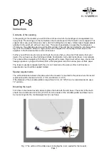
background image

DX-SX1H

– 1 –

• In the interests of user-safety the set should be restored to its

original condition and only parts identical to those specified be
used.

SERVICE MANUAL

SHARP  CORPORATION

No. S6053DXSX1H//

This document has been published to be used
for after sales service only.
The contents are subject to change without notice.

 CONTENTS

Page

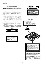
SAFETY PRECAUTION FOR SERVICE MANUAL ...........................................................................................................  2
IMPORTANT SERVICE NOTES (FOR U.K. ONLY) ..........................................................................................................  3
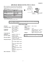
SPECIFICATIONS .............................................................................................................................................................  3
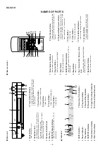
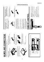
NAMES OF PARTS ...........................................................................................................................................................  4
OPERATION MANUAL ......................................................................................................................................................  5
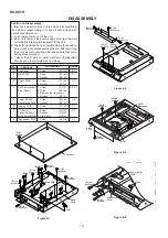
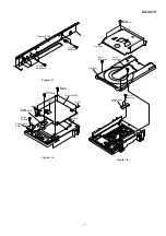
DISASSEMBLY ..................................................................................................................................................................  6
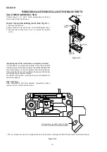
REMOVING AND REINSTALLING THE MAIN PARTS .....................................................................................................  8
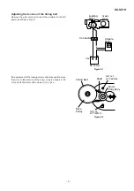
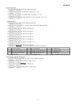
ADJUSTMENT .................................................................................................................................................................  10
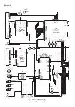
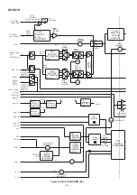
BLOCK DIAGRAM ...........................................................................................................................................................  12
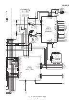
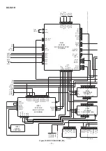
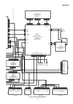
SCHEMATIC DIAGRAM / WIRING SIDE OF P.W.BOARD .............................................................................................  18
NOTES ON SCHEMATIC DIAGRAM ..............................................................................................................................  41
TYPES OF TRANSISTOR AND DIODE ..........................................................................................................................  41
FUNCTION TABLE OF IC ................................................................................................................................................  42
WIRING OF PRIMARILY SUPPLY LEADS (FOR U.K. ONLY) ........................................................................................  66
PARTS GUIDE/EXPLODED VIEW/PACKING METHOD (FOR U. K. ONLY)

DX-SX1H

MODEL

SACD PLAYER

Summary of Contents for DX-SX1H

Page 1: ...thout notice CONTENTS Page SAFETY PRECAUTION FOR SERVICE MANUAL 2 IMPORTANT SERVICE NOTES FOR U K ONLY 3 SPECIFICATIONS 3 NAMES OF PARTS 4 OPERATION MANUAL 5 DISASSEMBLY 6 REMOVING AND REINSTALLING THE MAIN PARTS 8 ADJUSTMENT 10 BLOCK DIAGRAM 12 SCHEMATIC DIAGRAM WIRING SIDE OF P W BOARD 18 NOTES ON SCHEMATIC DIAGRAM 41 TYPES OF TRANSISTOR AND DIODE 41 FUNCTION TABLE OF IC 42 WIRING OF PRIMARILY S...

Page 2: ...ept for U K LASER KLASSE 1 LUOKAN 1 LASERLAITE KLASS 1 LASERAPPARAT VAROITUS LAITTEEN KÄYTTÄMINEN MUULLA KUIN TÄSSÄ KÄYTTÖOHJEESSA MAI NI TULLA TAVALLA SAATTAA ALTI STAA KÄYTTÄJÄN TURVALLI SUUSLUOKAN 1 YLITTÄVÄLLE NÄKYMÄTTÖMÄLLE LASERSÄTEILYLLE VARNING OM APPARATEN ANVÄNDS PÅ AN NAT SÄTT ÄN I DENNA BRUKSANVI SNI NG SPECI FI CERAS KAN ANVÄNDAREN UT SÄTTAS FÖR OSYNLIG LASERSTRÅLNING SOM ÖVERSKRIDER ...

Page 3: ... lamp lights NG The NG lamp lights and the buzzer sounds SHORT CIRCUIT AC POWER SUPPLY CORD CONNECT THE PROBE TO GND OF CHASSIS SCREW PROBE AC UNIT WITHSTANDING VOLTAGE TESTER OUT Channel Stereo 2 channels Frequency range 2 Hz 100 kHz Super Audio CD Frequency 2 Hz 50 kHz response Super Audio CD 2 Hz 20 kHz CD Total harmonic distortion 0 0012 1 kHz 2 V Dynamic range 105 dB or more Super Audio CD Wo...

Page 4: ...SACD Indicator 2 Pause Indicator 3 Play Indicator 4 SACD CD Indicators 5 Track Number Indicator 6 Total Time Indicator 1 Direct Selection Buttons Used to select tracks directly 2 Program Button Used to change the order of tracks 3 Clear Button Clears the programmed tracks 4 SACD CD Selector Button Used to set the mode to SACD or CD on a hybrid disc 5 Stop Button Stops the disc 6 Fast Forward Fast ...

Page 5: ...plifier Use the point of a ball point pen or the like to switch Conventional amplifiers and speakers are de signed to meet the audible range If the vol ume or tone level of your amplifier is turned up too high during playback noise may be generated or the protection circuit may be activated Set this switch according to the amplifier to be connected to prevent the above prob lems Setting to CUSTOM ...

Page 6: ... 3 1 Top Panel 1 Screw A1 x5 6 1 2 Main PWB 1 Screw B1 x10 6 1 2 Socket B2 x6 3 Power PWB 1 Screw C1 x6 6 1 2 Socket C2 x5 4 SACD Mechanism 1 Screw D1 x7 6 2 6 3 Front Panel 2 Screw D2 x8 3 Remove the tray cover 4 Socket D3 x1 5 Power Switch 1 Screw E1 x5 6 4 Headphones PWB 2 Socket E2 x2 6 Display PWB 1 Screw F1 x7 7 1 7 CD Servo 1 Screw G1 x7 7 2 Pickup Sensor 2 Socket G2 x3 Mode Switch PWB 3 Fl...

Page 7: ...1 x2 ø2x5mm F1 x5 ø2 6x8mm Display PWB G1 x1 ø1 7x3mm G1 x4 ø3x6mm G1 x2 ø2x5mm G3 x1 G3 x1 G2 x1 G2 x2 CD Servo PWB Pickup Sensor PWB Mode Switch PWB H1 x4 ø2 6x6mm H1 x1 ø2 6x6mm H1 x2 ø2x5mm H1 x2 ø2 6x6mm Top Plate Tray Ass y Tray Sensor PWB ...

Page 8: ...cts It is necessary to position the spindle motor the sub shaft mechanism and the pickup to play a nonstandardized SACD disc If the pickup or motor is replaced at the service division these adjustments cannot be performed because of the facility and measuring equipment matters The SACD mechanism completed products are adjusted for the above reasons After installing After installing the SACD mechan...

Page 9: ...DC Power 3 5V M 1 2 Loading Motor Gear Unit Connector Ampere Meter Figure 9 1 If measurement of the loading motor current is possible move the motor in the direction of the arrow so as to obtain 40 50 mA and fix the motor with screws A1 x 2 pcs A1 x1 ø1 7x2mm A1 x1 ø1 7x2mm Timing Belt Shaft Motor Pully Ass y Drive Pulley Figure 9 2 ...

Page 10: ...1 0 _ 9 0 9 2 8 Year Month Day 2Model number Press the PLAY button in the step 1 Display 1 0 _ 0 0 0 1 0 Model number 3Version Press the PLAY button in the step 2 Display 1 0 _ A 0 0 0 1 Version number 4Then press the PLAY button to return to the initial test mode Display F 0 _ 0 0 0 0 0 4 Mechanism test 1 In case of the no disc mode eject the tray Display 2 0 _ 0 0 0 0 0 2Tray mechanism aging mod...

Page 11: ...s the PLAY button in the step 5 Display 3 2 5 0 0 0 0 0 7Next step Press the PLAY button in the step 6 Display 3 2 6 0 0 0 0 0 8Next step Press the PLAY button in the step 7 Display 3 2 7 0 0 0 0 0 9Next step Press the PLAY button in the step 8 Display F 1 1 Automatic adjustment values are displayed 8 Continuous playback test mode 1Enter the continuous playback test mode from the dynamic test mode...

Page 12: ...3 21 24 25 20 22 M MECSW EJ SW LD SW MECSW2 LD FWD LD RVS IN SW DFCT SEEK CHOP OFTRK TE LVL FE RFRP SLING SLIN 25 OPIN OPOUT OPIN 1 27 28 VREF Vref 5 5 6 6 1 6 4 4 5 3 4 3 4 3 3 3 3 4 4 23 19 22 20 FO IN TR ING FO ING TR IN SS ECR 5 7 4 LD CTL 6 LD RVS MUTE LD FWD LD SL LD SL 14 10 13 11 VDD 3 12 54 49 47 50 46 P1TP VREF_IN 18 16 17 TR FO TR FG 12 GAIN2 GAIN0 SPIN FG GAIN1 DVD_L 27 25 28 24 21 22 ...

Page 13: ...24MHz 54MHz 9 3 4 5 12 13 14 INV Buff Vref TO IC901 WARF TP506 4 LDO2 45 LDO1 4 DOUT DMO 52 51 48 23 RAS 8 WE 22 7 OE RVDD RASN 53 47 55 MWEN 56 ED7 CK54M 3 CK27M 32 24 1 PLCK RF Vref TE AGND TP510 FE TP507 TP509 TP508 TP513 PLCK DATA DGND TP511 TP512 52 SEL Vref STCK STDA 97 98 D 9 10 11 23 22 HCEN HDRD H1 0 HINT SD0 90 89 85 79 21 SERR 8 SOSO SD7 HDWT SDCK RSTN SVAL SREQ 91 92 94 95 24 32 100 3 ...

Page 14: ... 17 21 I O1 I O3 I O4 I O8 A16 A0 12 23 25 CE1 29 24 22 R W OE 53 BUFD0 EXPPAU2 61 26 55 BUFC0 SBUFB0 24 HADR 47 46 44 38 45 EXPD0 EXPC0 EXPD2 EXPC5 EXPD1 HDATA7 6 5 HRD 8 15 HWR HCS EXPPAU3 BUFD1 27 58 56 SBUFAI SBUFAO SBUFB1 59 54 57 CHOP LD_RVS OFTRK LD_SW EJ_SW IN_SW LD_FWD DFCT 48 39 34 D0 D3 D4 D11 D12 D15 16 7 2 A0 A3 A4 A11 A12 A23 117 31 MSDATO 91 SMUTE ECCINT ECC_CS XMSREDY 66 89 90 XMSL...

Page 15: ... 256FS CDFRM CDCLK CDDAT CNP901 D_GND DOUT D5V RXDA RXDCTL IC901 CXD2751Q SACD PLAYBACK SIGNAL PROCESSOR IC903 16Mbit SDRAM IX2840AF D_GND AT5V D_GND FIL AT 30V FIL KEY2 FIP_DA DISPLAY R C FIP_CK FIP_CS KEY1 AT5V TO DISPLAY CNP903 13 TO POWER A_5V FIL AT5V FIL AT8V AT 30V M_GND A_GND D_GND D3 3V H D3 3V L D5V VM RP 12 CE OE IC805 IX1539GE FLASH ROM 4M 8 16 24 25 28 A18 A0 29 36 38 45 WR D0 D16 IC8...

Page 16: ...X2838AF LINE AMP DSD CTL 73PIN MCK to TC9461 DVD L BCKA DSAR DSAL BCKA IC324 TC74HCT08A 4x2 INPUT AND GATE IC325 TC74HCT08A 4x2 INPUT AND GATE IC303 5 7 2 1 6 5 33 8688MHz X301 IC328 TC7WU04U 3 CIRCUIT INVERTER IC318 IX2838AF LINE AMP IC307 IX2838AF LINE AMP IC306 IX2838AF LINE AMP IC304 DSD1700E DSD CONVERTER R CH L CH IC302 DSD1700E DSD CONVERTER IC327 IX2838AF LINE AMP IC326 IX2838AF LINE AMP P...

Page 17: ...8 NJM4580M HEADPHONES AMP IC301 SM6451AV VOLUME CONTROL SW207 OPEN CLOSE SW206 NEXT SW205 STOP SW204 PLAY SW203 PAUSE SW202 PREV SW201 SACD CD FL201 FL DISPLAY IC201 MN12510F FL DRIVER XLF201 4 000MHz FIX OUT VAR OUT RLY 3 KEY2 KEY1 DA CK CS RELAY SWITCHING 0V 50V J302 1BIT SOC301 RCA TERMINAL DIGITAL OUTPUT J301 OPTICAL FIBER DATA LINK SW301 FILTER L102 LINE FILTER F101 T1A L 250V SOC1 AC INLET A...

Page 18: ... 8 9 10 11 1 2 3 4 5 6 7 8 9 10 11 1 2 3 4 5 6 7 8 9 10 11 14 13 12 11 10 9 8 7 6 5 4 3 2 1 1 2 3 4 5 6 7 8 9 10 11 12 13 14 15 16 17 18 19 20 21 22 23 24 25 26 27 28 DATA 1 2 3 4 5 6 7 8 9 10 11 12 13 14 15 16 17 18 19 20 21 22 23 24 25 26 27 28 1 2 3 4 5 6 7 8 9 10 11 12 13 14 15 16 17 18 19 20 21 22 23 24 25 26 27 28 2 1 3 7 8 6 5 4 3 2 1 10 9 11 12 13 14 15 16 CNP906 TO SACD PWB P25 12 G 1 2 3...

Page 19: ...R459 56K R460 56K R458 47 IC318 IX2838AF LINE AMP C468 0 0027 R482 68 C426 10 16 C470 0 001 R495 1 5K R358 56K C350 0 001 Q303 2SC2878B C463 100 16 C464 100 16 R359 56K R356 470 C351 0 001 Q304 2SC2878 B D305 RB419D D304 RB491D CNP308 CNS101A CNS101B D306 DAP202K IC314 KIA7805API 5V VOLTAGE REGULATOR C360 0 01 C492 0 001 C480 0 001 C364 10 16 C372 100 25 CNP307 CNS307A CNS307B IC317 KIA7909PI 9V V...

Page 20: ...SACD PWB 1 2 3 4 1 2 3 4 11 12 13 14 1 2 3 1 2 3 1 2 3 TO MAIN PWB B B 0V 25 3V 25 8V 25 8V 25 7V 25 7V 28 5V 4 9V 4 6V 0V 5 0V 31 5V 25 1V 5 0V 0 2V 4 5V 4 0V 5 0V 5 0V 0V 0V 0V 0V 0V B B B B B B HEADPHONES PWB A3 DISPLAY PWB A2 CNP305 P19 12 B CNP903 1 2 UN201 REMOTE SENSOR GP1U271R R202 100 C211 47 6 3 CNP203 JAK201 HEADPHONES CNP202 C212 0 1 C214 150P CH C213 150P CH R215 1K R214 1K R213 1K XL...

Page 21: ... 39 40 41 42 43 44 1 2 3 4 5 6 7 8 9 10 11 12 13 14 15 16 17 18 19 20 21 22 23 24 28 5V 4 9V 4 6V 0V 0 4V 25 7V 25 7V 28 4V 28 5V 31 5V 5 0V 2 3V 2 4V 0V 4 0V 4 5V 0V 25 3V 19 1V 31 1V 31 1V 31 3V 22 2V 19 4V 22 4V 28 5V 28 5V 28 4V 28 3V 28 3V 28 6V 25 3V 24 2V 28 4V 28 4V 0 4V 13 1V 19 4V 19 4V 28 4V 19 4V 28 4V 16 2V 25 3V 28 1V 31 3V 5 0V B B B B B B B SACD PLAY 3 1 2 R218 33K R219 33K R220 33...

Page 22: ...5 6 7 8 9 10 11 12 13 CNS101B P19 10 G RP10 0 7 Posis C136 0 1 C137 0 1 RP102 0 7 Posistor C129 0 1 C128 0 1 D108 D4SBS6 C133 0 1 F102 T2A L 250 C134 0 1 F103 T2A L 250 C126 0 1 C125 0 1 D109 D4SB60L RP107 0 7 Posistor IC102 BP5220 DC DC CONVERTER C 10 C127 47 25 RP106 C124 100 25 C119 0 1 ML DZ113 MTZJ9 1B C120 0 022 R183 220 R184 470 Q118 2SC1740 SR Q117 2SD2061 F C110 47 25 C111 100 16 C105 0 0...

Page 23: ...stic inner tube CNS105 CNP105 RP101 0 7 Posistor C136 0 1 C137 0 1 RP102 0 7 Posistor 9 D108 D4SBS6 C133 0 1 F102 T2A L 250V C134 0 1 F103 T2A L 250V D109 D4SB60L 07 tor IC102 BP5220 DC DC CONVERTER C140 100 25 27 25 C118 0 01 C123 33 50 R187 33K DZ114 HZS30L3 C130 0 01 R190 100 C135 10 50 R191 1 5K 1 2W Q121 KTA1266 GR 30V VOLTAGE REGULATOR C138 220 50 L102 LINE FILTER F101 T1A L 250V CNP107 CNS1...

Page 24: ...2 13 14 15 11 17 18 19 10 16 36 37 38 39 40 31 32 33 34 35 46 47 48 49 50 41 42 43 44 45 56 57 58 59 60 51 52 53 54 55 61 62 63 64 65 66 67 68 69 70 71 72 73 74 75 76 77 78 79 80 81 82 83 84 85 86 87 88 89 90 5 4 3 2 1 7 8 9 6 12 13 14 11 10 22 23 24 25 21 27 28 29 20 26 30 15 17 18 19 16 5 5 4 4 3 3 2 2 1 1 7 8 9 6 12 13 14 11 10 15 16 44 45 46 47 48 42 41 40 43 37 36 35 38 39 34 33 1 1 32 48 92 ...

Page 25: ...2 R C FIP_DA FIP_CK FIP_CS KEY1 AT5V B B B B B B B B B B B B B B B B B B B B B B B B SACD PWB C 1 2 5 5 4 4 3 3 2 2 1 1 7 7 8 8 9 9 6 6 12 13 14 15 16 17 18 19 20 21 22 23 24 25 66 67 68 69 70 61 62 63 64 65 76 77 78 79 80 71 72 73 74 75 56 57 58 59 60 51 52 51 52 53 54 55 26 27 28 81 81 82 83 84 85 86 87 88 89 90 91 92 93 94 95 96 97 98 99 100 11 11 12 13 14 15 16 17 18 19 20 10 5 4 3 2 1 2 1 7 8...

Page 26: ...11 10 TRAY SENSOR PWB D1 MODE SWITCH PWB D2 PICKUP IN SENSOR PWB D3 Q501 2SA1037 KR R519 4 7K Q502 DTC144 EK C516 0 01 R518 2 2K R521 47 R527 47 Q503 2SA1955 A C523 47 10 R529 470 C527 0 01 D505 DAP202K R541 47 R542 47 C529 47 10 Q504 2SA1955 A R545 470 L501 10µH R563 10K C5 0 C531 0 01 C532 0 1 C528 47 6 3 C520 0 1 C524 0 1 R534 39K C519 0 1 R524 5 6K R523 5 6K R528 1 C506 1 C505 1 C504 1 C503 1 ...

Page 27: ...P C621 0 01 C620 1 C618 1 C619 0 01 C617 22P CH C615 0 033 C616 0 01 R619 270K C605 0 1 C606 100 6 3 C601 470P R602 5 6K C607 330P CH R601 10K R607 15K R604 10K C610 330P CH R616 470 R615 470 R608 220K R618 1K C562 0 1 C563 0 0047 C564 0 0047 C565 0 1 C566 0 1 C567 0 1 C560 1 C554 0 001 Q505 DTC144 EK C555 0 0022 C552 0 001 C549 0 001 C551 0 001 C546 22 6 3 C543 0 001 C547 0 1 C544 47 6 3 R581 3 3...

Page 28: ...5 46 47 48 49 50 51 52 53 54 55 56 57 58 59 60 61 62 63 64 65 66 67 68 69 70 71 72 73 74 75 767778798081828384858687888990919293949596979899100 1 2 3 14 15 16 1 2 3 4 5 6 7 8 1 2 3 4 5 6 7 8 1 2 3 4 19 5 6 7 8 9 18 17 16 15 14 13 12 11 10 20 21 22 23 24 25 26 27 28 29 30 31 32 33 34 35 36 37 38 39 40 41 42 43 44 45 46 47 48 49 50 51 52 53 54 55 1 62 61 60 59 58 57 63 56 64 65 66 67 68 69 70 71 72 ...

Page 29: ...16 C121 R177 Q119 IC103 C106 R178 R181 C109 R185 R188 C131 CNP101 R184 RP106 C110 C105 Q117 Q118 C111 R183 DZ113 C120 C119 C124 RP105 CNP102 DZ115 C139 D101 RP108 C138 DZ114 C135 C130 R190 R191 R187 C123 C118 IC101 C104 C108 Q121 BI101A SW101 POWER C145 1 2 1 2 1 2 3 4 5 6 7 8 9 10 11 12 13 1 2 3 4 5 6 7 8 9 10 11 12 13 1 2 3 4 5 6 7 8 9 10 11 12 13 8 7 6 5 4 3 2 1 8 7 6 5 4 3 2 1 8 7 6 5 4 3 2 1 ...

Page 30: ...9 R464 IC321 R463 C487 C372 C397 C492 J301 OPTICAL FIBER DATA LINK SOC301 RCA TERMINAL SOC302 LINE OUTPUT TERMINAL J302 1BIT TERMINAL 3 2 1 4 3 2 1 1 2 3 4 5 6 7 8 9 10 1 2 3 4 5 6 7 8 9 10 8 7 6 5 9 10 11 13 12 14 C389 C388 R343 IC308 C379 C368 C411 C347 R390 C338 C367 C357 C366 IC301 C333 C410 C C374 IC317 D305 C4 C369 IC316 C396 CNP308 IC312 R404 IC309 Q313 E C B E C B E C B E C B 1 2 1 3 4 5 8...

Page 31: ...14 R318 C450 C452 R332 C451 R329 R366 R365 R362 C311 C329 C332 C323 C317 R363 R309 C320 C324 C321 C316 C325 CNP302 IC302 R301 R303 C309 R352 C310 C318 BI301A IC324 IC303 CNP301 C354 C330 C326 C322 X301 R436 R435 C405 C355 C335 C328 C306 R304 C307 IC328 C472 R496 L301 C406 C327 IC323 IC305 R317 E E C C B B 8 7 6 5 121110 9 4 3 2 1 8 7 6 5 121110 9 4 3 2 1 8 7 6 5 121110 9 4 3 2 1 1 2 3 4 5 6 7 8 1 ...

Page 32: ...47 C358 C383 R459 R457 R449 R479 R399 C334 R379 C3 R482 R367 R460 R360 R458 R364 R361 R391 R493 R349 CK57 CK60 CK99 CK187 CK91 CK181 CK89 CK67 CK185 CK68 CK148 CK130 CK90 CK69 TP310 CK77 CK131 CK76 TP306 CK75 CK132 CK78 CK133 TP303 CK74 CK65 TP304 CK117 CK66 CK72 CK73 CK118 CK149 CK64 CK71 CK63 CK156 CK119 CK62 CK146 CK120 CK145 CK61 CK158 CK126 CK153 CK128 CK179 TP302 TP301 CK147 CK127 TP309 CK12...

Page 33: ...C475 C433 C434 R468 R415 R429 R473 MAIN PWB A1 BOTTOM VIEW R349 Q316 CK6 CK186 CK3 CK4 CK10 CK21 CK12 CK11 CK23 CK20 CK22 CK56 CK9 CK159 CK55 CK8 CK7 CK54 CK5 CK162 CK163 CK166 CK53 CK164 CK182 CK184 CK50 CK19 CK171 CK49 CK79 CK167 CK174 CK18 CK17 CK16 CK48 CK15 CK52 CK51 CK14 CK47 CK13 CK57 CK60 CK178 CK183 CK137 CK138 CK135 CK139 CK136 CK134 CK59 CK140 CK173 CK141 CK58 CK144 CK175 CK177 CK143 CK...

Page 34: ...0 C570 C572 C571 R612 C515 C672 C513 C514 C626 R502 CNS502 R501 R533 CNP505 R647 C660 R643 R642 R644 C666 R614 C607 R608 R601 R602 C601 1 1 1 1 1 8 5 3 5 3 CNS51B P40 3 G TO PICKUP IN SENSOR PWB TO SPINDLE MOTOR CNS52B P40 3 C TO TRAY SENSOR PWB CNS53B TO MODE SWITCH PWB TO PICKUP TO MAIN PWB CNS307B CNS302B TO MAIN PWB P30 4 A TO MAIN PWB CNS309B 1 5 10 14 15 20 25 28 SACD PWB C TOP VIEW 11 1 80 ...

Page 35: ... R507 C512 IC503 R503 C511 D504 C508 C501 D501 R504 D502 C502 D503 C510 IC804 CNP501 IC801 CNP904 C918 R647 C660 R643 C509 R642 R644 C666 614 C607 R608 R601 R602 C601 R549 R574 C574 R592 C539 TO SPINDLE MOTOR P30 4 A TO MAIN PWB CNS309B TO SLED MOTOR TO POWER PWB CNS102B TO DISPLAY HEADPHONES PWB CNS201A TO LOADING MOTOR 1 11 1 13 1 5 10 12 13 1 4 15 20 24 1 5 10 15 16 17 20 25 30 32 1 4 5 8 1 14 ...

Page 36: ...R571 IC506 IC507 R648 R582 R583 R852 C814 R842 R841 R840 R833 R816 R815 R832 R814 R813 R812 R811 R810 R822 C809 R830 R827 R826 C808 C802 R821 R823 R808 R809 C806 C545 C810 R835 C811 R863 R856 R858 R857 R913 L901 R910 R838 R860 R859 R865 R834 R831 R828 R836 C812 Q801 R804 R802 R844 R845 R843 R803 R872 R871 R806 R805 R817 R870 C820 R869 R848 R855 C819 IC805 R849 R846 R854 C817 C818 R853 R929 C816 R8...

Page 37: ...5 R909 R908 C910 IC902 R907 C908 R936 R905 CNP906 C638 C641 R629 C639 C634 C633 C625 C604 C614 R609 R620 R624 R625 C635 R630 R934 R933 R589 R580 R593 R590 R563 R528 C506 C505 Q505 C560 C558 C554 C552 C551 C553 C549 R581 C547 C540 C548 R529 D505 C532 R527 R521 C531 Q503 R519 C527 R541 R542 Q504 R545 C555 C556 Q506 C543 C919 R513 R506 R505 R50A Q502 R518 Q501 R801 C902 R922 1 5 10 11 15 R920 R917 R9...

Page 38: ...3 34 35 40 44 OP IC201 FL201 D201 D203 Q203 R216 R210 C205 R212 C203 R225 R217 R218 R219 R220 R221 R222 R223 R226 Q204 DISPLAY PWB A2 TOP VIEW DISPLAY PWB A2 BOTTOM VIEW 1 5 10 15 20 25 30 35 40 45 50 CK37 CK26 CK36 CK35 CK34 CK33 CK32 CK57 CK29 CK31 CK30 CK56 CK25 CK24 CK54 CK53 CK52 CK51 CK50 CK49 CK47 CK46 CK44 CK28 CK55 CK48 CK45 CK43 CK42 CK41 CK38 CK40 CK13 CK21 CK39 ...

Page 39: ...PWB A3 TOP VIEW HEADPHONES PWB A3 BOTTOM VIEW CNP203 CNP202 C212 C213 C214 R202 C211 JAK201 HEADPHONES TERMINAL UN201 BR RD OR YL GR BL VL GY WH BK BR RD OR OR RD BR CNP903 CNS201C TO SACD PWB CNP305 P30 5 B TO MAIN PWB CNS201A CNS201B BR RD OR YL GR BL VL GY WH BK CNS202A CNS202B R213 R214 BR COLOR TABLE RD R OR YL GR BL VL GY WH W BK PK BROWN RED ORANGE YELLOW GREEN BLUE VIOLET GRAY WHITE BLACK ...

Page 40: ... PICKUPIN SENSOR PWB D3 BOTTOM VIEW CNP53 CNS53A CNS53B SW51 PLAY SW52 STOP 3 2 1 3 2 1 3 2 1 CNP505 P34 2 D TO SACD PWB CNP504 P34 2 B TO SACD PWB CNP52 CNS52A CNS52B 1 2 3 4 5 1 2 3 4 5 1 2 3 4 5 CNP51 CNS51A CNS51B CNP503 P34 3 A TO SACD PWB CNP501 P35 10 H TO SACD PWB CNP502 P35 11 B TO SACD PWB 1 2 3 1 2 3 1 2 3 CNS501 P34 2 C TO SACD PWB CNS502 P34 6 A TO SACD PWB FLEXIBLE PWB SLED MOTOR RD ...

Page 41: ...one with Fusible is a fuse type Capacitor To indicate the unit of capacitor a symbol P is used this symbol P means micro micro farad and the unit of the capacitor without such a symbol is microfarad As to electrolyticcapacitor theexpression capacitance withstand voltage is used CH TH RH UJ Temperature compensation ML Mylar type P P Polypropylene type Schematic diagram and Wiring Side of P W Board ...

Page 42: ... between VPP terminals 39 42 P10 P13 High tension output Output 4 bit high tension output port SEG8 SEG11 Can be switched to general purpose output segment output by bit unit Output type is Pch open drain 43 44 P20 P23 High tension output Input Output 4 bit high tension output port 1 2 DGT12 SEG15 Can be switched to general purpose input general purpose output DGT15 SEG12 segment output digit outp...

Page 43: ...L channel audio input 7 AVDD Analog VDD 8 VRL Output Capacity connecting terminal for L channel reference voltage VDD 2 9 VRR Output Capacity connecting terminal for R channel reference voltage VDD 2 10 AVSS Analog VSS 11 RIN Input R channel audio input 12 ROUT Output R channel audio output 13 DVSS Digital VSS 14 MLEN Input terminal with pull up Microcomputer latch enable input 15 MCK Input termin...

Page 44: ...Output Analog output from DAC Hot positive 17 18 AGND Analog ground 19 VCC Analog power supply 5V 20 AGND Analog ground 21 22 VCC Analog power supply 5V 23 AGND Analog ground 24 VCC Analog power supply 5V 25 AGND Analog ground 26 DATA Input Direct stream digital data input 27 DCK Input Data clock input 28 SCK Input System clock input Pin No Terminal Name Input Output Function 1 2 3 4 5 6 7 8 9 10 ...

Page 45: ...ut amplifier common 19 AGND2L Analog GND 20 VCC2L Analog power supply 5V 21 ZERO Output Zero data flag 22 RST Input Reset While this pin is in L DF and delta sigma modulator are in the reset condition 23 CS IWO Input Chip select input format select 24 MODE Input Mode control select H software L hardware 25 MUTE Input Mute control 26 MD DM0 Input Mode control data de emphasis select 1 27 MC DM1 Inp...

Page 46: ...utput RF ripple peak 28 RFO Output Equalizing RF output 2 3 V 29 30 NC NC terminal Used by connecting to GND 31 VCCR Power terminal RF 32 DPDB Input Pit depth adjustment VrD DPDB increase brings delay capacity increase on sides A and B 33 TEB Input TE balance VrD TEB increase brings increase in gain on TP side and in delay capacity on sides A and C 34 FEB Input FE balance VrD FEB increase brings i...

Page 47: ... Output Function Terminal DC Voltage TYP Remarks P1FN P1FP LDP1 P1DI P1CI P1BI P1AI GNDR LDP2 P2AI P2BI P2CI P2DI GNDS P2FP P2FN DPDB VccR NC NC RFO RPP RPB RPO RPZ VccS DFTN FEO TEO LVL LccP VCKF NC P1TP P1TN LDO1 MDI1 EQF EQB RFA RFDC GND2 EQD NC Vcc2 PSC FEB TEB GND P2TP P2TN LDO2 MDI2 VrA VrD Vdd DPAC DPBD DPD1 DPD2 SCB SCL SCD SRCK 1 2 3 4 5 6 7 8 9 10 11 12 13 14 15 16 17 18 19 20 21 22 23 2...

Page 48: ...cillation frequency set terminal Capacitor is externally mounted 23 CW CCW Clockwise counterclockwise input 24 CK2 Clock signal input Pin No Terminal Name In this unit the terminal with asterisk mark is open terminal which is not connected to the outside Function Figure 48 BLOCK DIAGRAM OF IC 7 VCC 5 MO 17 16 13 YMA ØA ØA IA 14 NFA 8 VMB 12 9 ØB 11 10 NFB ØB IB PG B POWER GROUND B 15 PG A POWER GR...

Page 49: ...s terminal 21 VM Motor power terminal 8 H3 Hall element 3 positive input terminal 22 CS1 Current detection terminal 1 9 H3 Hall element 3 negative input terminal 23 NC Not used 10 SS Start Stop switching terminal 24 NC Not used 11 TFLG Thermal protection monitor terminal 25 NC Not used 12 FG FG signal output terminal 26 A3 Drive output 3 13 BRK Break mode set terminal 27 A2 Drive output 2 14 NC No...

Page 50: ...input terminal 21 VCC VCC 8 TRAY IN Tray input terminal 22 CH2 IN CH2 input terminal 9 GND Substrate GND 23 CH2 IN CH2 gain adjustment input terminal 10 CH5 OUT Tray negative output terminal 24 CH3 IN CH3 input terminal 11 COM OUT Tray positive terminal CH4 negative output terminal 25 CH3 IN CH3 gain adjustment input terminal 12 CH4 OUT CH4 positive output terminal 26 VREF IN Bias amplifier input ...

Page 51: ...er 38 LPFO Output Output of amplifier for PLL loop filter 39 VCOF Output VCO filter terminal 40 SCLO Output Reference voltage output terminal of built in comparator 41 AVSS Analog power supply 0V 42 AVR Output Non PLL analog reference potential 1 65V 43 VRC Resistance dividing point potential For generating analog reference potential 1 65 44 PVR Output PLL analog reference potential 1 65V 45 AVDD ...

Page 52: ... 100 DVSS Digital power supply 0V For logic cell Pin No Terminal Name Input Output Function Remarks IC603 VHiSC514870SJ 4Mbit DRAM SC514870SJ Pin No Terminal Name Function 10 13 16 20 9 A0 A8 A9R Address input 8 RAS Row address strobe 23 CAS Column address strobe 2 5 24 27 DQ1 DQ8 Data input Data output 22 OE Output enable 7 WE Write enable 1 VCC Power supply 5V 15 28 VSS Ground 0V 6 21 NC Not use...

Page 53: ...y shift terminal 22 PDOS Output Phase error between EFM and PLCK signal output terminal to be used in case of 8 time speed operation 23 PDO Output Output terminal for phase error signal between EFM signal and PLCK signal 24 TMAXS Output TMAX detection result output terminal Selected by command bit TMPS 25 TMAX Output 26 LPFN Input Inversion input terminal of amplifier for low pass filter 27 LPFO O...

Page 54: ...om IO0 and 1 terminals and disc equalizer binary PWM from IO2 and 3 terminals L active 64 CKSE X tal select terminal In case of 16 9344MHz H in case of 33 8688 MHz L 65 DACT Test terminal 66 TESIN Input Test input terminal 67 TESIO1 Input Output Test input output terminal 68 VSS Digital ground terminal 69 PXI Input DSP system clock oscillation circuit input terminal 70 PXO Output DSP system clock ...

Page 55: ...l which is not connected to the outside UHSO H H Normal speed playback H L Double speed playback L H 4 time speed playback L L 8 time speed playback HSO Playback speed 76 DVDD 77 RO 78 DVSS 79 DVR 80 LO 81 DVDD 82 TEST1 83 TEST2 84 TEST3 85 BUS0 86 BUS1 87 BUS2 88 BUS3 89 VDD 90 VSS 91 BUCK 92 CCE 93 TEST4 94 TSMOD 95 RST 96 TEST0 97 HSO 98 UHSO 99 EMPH 100 LRCX 50 DMO 49 FVO 48 FMO 47 TEBC 46 RFG...

Page 56: ...TCLKA P1 3 PO11 TIOCD0 TCLKB P1 4 PO12 TIOCA1 P1 5 PO13 TIOCB1 TCLKC P1 6 PO14 TIOCA2 P1 7 PO15 TIOCB2 TCLKD P2 0 PO0 TIOCA3 P2 1 PO1 TIOCB3 P2 2 PO2 TIOCC3 P2 3 PO3 TIOCD3 P2 4 PO4 TIOCA4 P2 5 PO5 TIOCB4 P2 6 PO6 TIOCA5 P2 7 PO7 TIOCB5 P4 7 AN7 DA1 P4 6 AN6 DA0 P4 5 AN5 P4 4 AN4 P4 3 AN3 P4 2 AN2 P4 1 AN1 P4 0 AN0 V ref AV cc AV ss PA5 A21 IRQ5 PA4 A20 IRQ4 PA3 A19 PA2 A18 PA1 A17 PA0 A16 PB7 A15...

Page 57: ... 1 bit amplifier 35 EXPBU1 MECSW1 Input Tray position detection input 36 EXPBU2 MECSW2 Input Mechanism stop mode detection input 37 EXPBU3 SMODE Input Operating mode set input Opened S MODE 38 EXPC0 DVD_L Output SACD disc inserted CD stopped L 39 EXPC1 SMUTE Output Soft mute signal for SACD decoder 40 EXPC2 AMUTE Output Audio mute In case of playback manual search 41 VSS Digital GND 42 EXPC3 Input...

Page 58: ...2 41 40 39 38 37 36 35 34 33 1 2 3 4 5 6 7 8 9 10 11 12 13 14 15 16 31 30 29 28 27 26 25 24 23 22 21 20 19 18 17 VDD EXPD 3 EXPD 4 EXPD 5 BUFDO BUFDI SBUFBO SBUFBI SBUFAO SBUFAI MRST MODE BUFCO TEST BUFCI VSS VSS EXPBL 3 EXPBL 2 EXPBL 1 EXPBL 0 EXPAU 3 EAPAU 2 VDD VSS EXPAU 1 EXPAU 0 EXPAL 3 EAPAL 2 EXPAL 1 EAPAL 0 VDD VSS Q2 3 Q2 2 Q2 1 Q2 0 Q1 7 Q1 6 VDD VSS Q1 5 A1 4 Q1 3 Q1 2 Q1 1 Q1 0 VDD VDD...

Page 59: ...al Name In this unit the terminal with asterisk mark is open terminal which is not connected to the outside Function A4 CE A5 A6 A7 A8 A12 A13 A14 A15 A16 I O1 I O8 OE R W CE1 CE2 MEMORY CELL ARRAY 1024 x 28 x 8 1048576 VDD GND CE A0 A1 A2 A3 A9 A10 A11 CE ROW ADDRESS BUFFER ROW ADDRESS REGISTER ROW ADDRESS DECODER DATA CONTROL CLOCK GENERATOR SENSE AMPLIFIER COLUMN ADDRESS DECODER COLUMN ADDRESS ...

Page 60: ...n x 8 mode DQ15 A 1 address 31 DQ1 Input Output Lower byte data input output Data and command input during cycle of writing command user interface Memory array identifier and status data output when reading various data Float condition in case of chip non select or output disable 32 DQ9 Input Output Upper byte data input output The function is the same as shown in case of the lower byte data input...

Page 61: ...d status data output when reading various data Float condition in case of chip non select or output disable 45 DQ15 Input Output Upper byte data input output The function is the same as shown in case of the lower byte data input output above Operating only in x16 mode Floating in x 8 mode DQ15 A 1 address 46 GND Ground 47 NC Not used 48 A16 Input Block select addresses Select 1 32 erase block Thes...

Page 62: ...5 VSS Ground terminal 16 CK75S Input Master clock select terminal Selects H in case of 768Fs and L in case of 512Fs 17 EXCKO1 Output External output clock terminal 1 Outputs 768Fs 512Fs 256Fs 128Fs according to setting 18 EXCKO2 Output External output clock terminal 2 Outputs 768Fs 512Fs 256Fs 128Fs according to setting 19 LRCK Input Output IFs 44 1kHz clock input output terminal Selects master sl...

Page 63: ...cting PSP physical disc mark Inputs 27 00MHz 81 WRFD Input RF data input terminal for detecting PSP physical disc mark Inputs RF data made binary by slicer 82 WAD0 Input A D data input output terminal for detecting PSP physical disc mark LSB 83 88 WAD1 WAD6 Input A D data input output terminal for detecting PSP physical disc mark 89 WAD7 Input A D data input output terminal for detecting PSP physi...

Page 64: ...erminal Connected to 3V voltage power 14 VREF Positive reference voltage input terminal Voltage of this terminal ranges from 0 75V to VA 15 PD CMOS TTL compatible digital input terminal When this terminal is set to High ADC08351 enters the power down mode minimizing power consumption When this is set to Low the device enters the normal operation mode 16 VA Positive analog power voltage terminal To...

Page 65: ...14 28 27 26 25 24 23 22 21 20 19 18 17 16 15 VCC DQ1 DQ2 DQ3 DQ4 WE RAS NC A10R A0 A1 A2 A3 VCC VSS DQ8 DQ7 DQ6 DQ5 CAS OE A9 A8 A7 A6 A5 A4 VSS 1 2 3 4 5 6 7 8 9 10 11 12 13 14 28 27 26 25 24 23 22 21 20 19 18 17 16 15 VCC DQ1 DQ2 DQ3 DQ4 WE RAS NC A10R A0 A1 A2 A3 VCC VSS DQ8 DQ7 DQ6 DQ5 CAS OE A9 A8 A7 A6 A5 A4 VSS 28 pin plastic SOJ 28 pin plastic TSOP Type K 10 10 10 11 1 8 8 8 8 8 8 DQ1 DQ8 ...

Page 66: ...ect the 2 pin lead from BI101 under the PWB via the nylon band A Passing through the electrolytic condensers Tie the 2 pin lead at the back of the PWB Tie the 8 pin lead and the 10 pin lead at the two positions Main PWB CNP308 Tie the 2 pin lead at the back of the PWB 2 Pin lead connected from BI101 Make the 2 pin lead as tight as possible POWER SW BI101 POWER PWB BI101 Connect the 2 pin lead via ...

Page 67: ... lead wire VC CY Square type without lead wire VC CZ Square type without lead wire VC J The 13th character represents capacity difference J 5 K 10 M 20 N 30 C 0 25 pF D 0 5 pF Z 80 20 If there are no indications for the electrolytic capacitors error is 20 Resistors VRD Carbon film type VRS Carbon film type VRN Metal film type VR MF Cylindrical type without lead wire VR MN Cylindrical type without ...

Page 68: ... NPN DTC144 EK Q503 504 VS2SA1955A 1 J AC Silicon PNP 2SA1955 A Q505 507 VSDTC144EK 1 J AB Digital NPN DTC144 EK Q601 VSDTA144EK 1 J AB Digital PNP DTA144 EK Q602 VSDTC144EK 1 J AB Digital NPN DTC144 EK Q801 VSDTC144EK 1 J AB Digital NPN DTC144 EK DIODES D101 VHD11ES4 1 J AB Silicon 11ES4 D108 VHDD4SBS6 1 J AH Rectifier Diode D4SBS6 D109 VHDD4SB60L 1 J AG Rectifier Diode D4SB60L D201 VHDDAP202K 1 ...

Page 69: ...K J AA 470 pF 50V C453 VCKYTV1EB104K J AA 0 1 µF 25V C454 VCFRED1HM102J J AD 0 001 µF 50V C455 VCKYTV1HB221K J AA 220 pF 50V C456 VCKYTV1EB104K J AA 0 1 µF 25V C457 VCFRED1HM102J J AD 0 001 µF 50V C458 VCKYTV1HB221K J AA 220 pF 50V C459 460 VCKYTV1EB104K J AA 0 1 µF 25V C461 462 VCKYTV1HB221K J AA 220 pF 50V C463 464 RC EZ0476GEZZ J AC 100 µF 16V Electrolytic C465 466 RC EZ0468GEZZ J AC 10 µF 16V ...

Page 70: ...02J J AA 1 kohm 1 10W R216 223 VRS TV2AB333J J AA 33 kohms 1 10W R224 VRS TV2AB471J J AA 470 ohms 1 10W R225 VRS TV2AB333J J AA 33 kohms 1 10W R226 VRS TV2AB222J J AA 2 2 kohms 1 10W R301 VRS TV2AB560J J AA 56 ohms 1 10W R302 VRS TV2AB330J J AA 33 ohms 1 10W R303 VRS TV2AB560J J AA 56 ohms 1 10W R304 VRS TV2AB221J J AA 220 ohms 1 10W R305 VRS TV2AB105J J AA 1 Mohm 1 10W R306 308 VRS TV2AB102J J AA...

Page 71: ...ohm 1 16W R610 VRS CY1JB330J J AA 33 ohms 1 16W R611 VRS CY1JB103F J AA 10 kohm 1 16W R612 VRS CY1JB681J J AA 680 ohms 1 16W R613 VRS CY1JB103J J AA 10 kohm 1 16W R614 VRS CY1JB330J J AA 33 ohms 1 16W R615 616 VRS CY1JB471J J AA 470 ohms 1 16W R618 VRS CY1JB102J J AA 1 kohm 1 16W R619 VRS CY1JB274J J AA 270 kohms 1 16W R620 VRS CY1JB103J J AA 10 kohm 1 16W R621 VRS CY1JB103F J AA 10 kohm 1 16W R62...

Page 72: ...FZZ J AN Cover Mechanism 309 PCUSG0705AFZZ J AC Rubber Vibration 312 PCUSG0699AFZZ J AC Rubber Vibration 313 PSHEZ1144AFZZ J AG Sheet Mechanism Cover 315 GCOVA3135AFM1 J Tray Ass y 316 LANGF1627AFFW J AL Bracket Tray Rack 317 LANGZ0371AFM1 J AR Motor Bracket Ass y 318 LCHSZ0306AFZZ J AZ Base Chassis 319 LHLDM1065AFZZ J AY Stabilizer 320 LHLDZ1785AFM1 J AH Tray Guide Bearing Ass y A 321 LHLDZ1786AF...

Page 73: ... ø3 2 ø5 1mm 626 XWHSN33 05080 J Washer ø3 3 ø5 0 8mm 627 XNESN30 24000 J Nut ø3mm ACCESSORIES PACKING PARTS 1 GLEGG0126AF00 J AG Leg Cushion 2 QACCB0113AFZZ J AY AC Power Supply Cord For U K 2 QACCE0106AFZZ J AW AC Power Supply Cord Except for U K 3 QCNWG0429AFZZ J BF Connection Cord 4 RRMCG0332AFSA J BD Remote Control 5 SPAKA2749AFZZ J AX Packing Add Right 6 SPAKA2750AFZZ J AX Packing Add Left 7...

Page 74: ...42 711 344 718x2 315 711 344 340 711x4 316 320 341 718x2 712 324 711 M703 710 329 711x2 317 719x2 328 715 711x4 716 327 326 318 711x2 SW52 SW51 711x2 325 325 303 301 309x2 701x2 312x2 701x2 714 319 322 345 323 346 709 713x2 PWB D2 PWB D1 717x2 717 717 717x3 343 705x2 313 308 PWB D3 ...

Page 75: ...12 213 224x2 624x2 230x6 PWB B1 PWB A2 PWB A3 PWB B2 FL201 214 201 607 227x3 620x2 216 620x2 620x2 604x2 620x2 604x2 604x2 615x2 222 602x4 602 614 242 PWB C 247 210 247 625 247 247 619 238 226x4 215 241 604x5 607x2 232x2 607x2 603x5 231 243 220 621 626 246 621 246 627 609x4 608x2 229 Q117 623x2 615 606x3 T101 221 619x2 245 621x3 621x4 619x2 204 239 228x2 605x2 232 615 237 236 236 235 237 236 236 2...

Page 76: ...pan SG SK 1 Leg Cushion GLEGG0126AF00 2 AC Power Supply Cord QACCB0113AFZZ 3 Connection Cord QCNWG0429AFZZ 4 Remote Control RRMCG0332AFSA 5 Packing Add Right SPAKA2749AFZZ 6 Packing Add Left SPAKA2750AFZZ 7 Packing Case SPAKC7105AFZZ 8 Leg Protection Material SPAKZ0546AFZZ 9 Polyethylene Bag Accessories SSAKA0226AFZZ 10 Sheet Unit SSAKH0330AFZZ 11 Resistration Card TCADN0104AFZZ 12 Warranty Card T...

Reviews: