1
DV-NC150U
S74W9DV-NC150
SERVICE MANUAL
In the interests of user-safety (Required by safety
regulations in some countries) the set should be
restored to its original condition and only parts
identical to those specified be used.
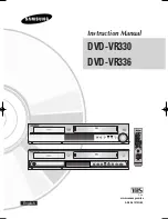
SERVICE MANUAL
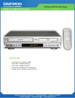
VCR/DVD COMBINATION
MODEL
DV-NC150U
VCR/DVD COMBINATION
This document has been published to be used for
after sales service only.
The contents are subject to change without notice.
SHARP CORPORATION
MAIN SECTION
1. SPECIFICATIONS ................................................................................................................................................ 1-1-1
2. LASER BEAM SAFETY PRECAUTIONS ............................................................................................................. 1-2-1
3. IMPORTANT SAFEGUARDS AND PRECAUTIONS ............................................................................................ 1-3-1
4. STANDARD NOTES FOR SERVICING ................................................................................................................ 1-4-1
5. PREPARATION FOR SERVICING ....................................................................................................................... 1-5-1
6. OPERATING CONTROLS AND FUNCTIONS ...................................................................................................... 1-6-1
7. CABINET DISASSEMBLY INSTRUCTIONS ........................................................................................................ 1-7-1
8. ELECTRICAL ADJUSTMENT INSTRUCTIONS ................................................................................................... 1-8-1
9. FIRMWARE RENEWAL MODE (FIRMWARE VERSION UP) .............................................................................. 1-9-1
10. TROUBLESHOOTING ........................................................................................................................................ 1-10-1
11. BLOCK DIAGRAMS ............................................................................................................................................ 1-11-1
12. FUNCTION INDICATOR SYMBOLS ................................................................................................................... 1-11-9
13. SCHEMATIC DIAGRAMS/ CBA’S AND TEST POINTS ..................................................................................... 1-12-1
14. WAVEFORMS & VOLTAGE CHART .................................................................................................................. 1-13-1
15. WIRING DIAGRAM ............................................................................................................................................. 1-14-1
16. SYSTEM CONTROL TIMING CHARTS .............................................................................................................. 1-15-1
17. IC PIN FUNCTION DESCRIPTIONS .................................................................................................................. 1-16-1
18. LEAD IDENTIFICATIONS ................................................................................................................................... 1-17-1
19. EXPLODED VIEWS ............................................................................................................................................ 1-18-1
20. MECHANICAL PARTS LIST ...............................................................................................................................
N/A
21. ELECTRICAL PARTS LIST ................................................................................................................................
N/A
DECK MECHANISM SECTION
1. STANDARD MAINTENANCE ............................................................................................................................... 2-1-1
2. SERVICE FIXTURE AND TOOLS ........................................................................................................................ 2-2-1
3. MECHANICAL ALIGNMENT PROCEDURES ...................................................................................................... 2-3-1
4. DISASSEMBLY / ASSEMBLY PROCEDURES OF DECK MECHANISM ............................................................ 2-4-1
5. ALIGNMENT PROCEDURES OF MECHANISM .................................................................................................. 2-5-1
6. DECK EXPLODED VIEWS ................................................................................................................................... 2-6-1
7. DECK PARTS LIST ...............................................................................................................................................
N/A
CONTENTS
MODEL
DV-NC150U
1
The region number for this
VCR/DVD is 1.