1
DV-NC100S/DV-NC100S(S)/DV-NC100S(Q)/DV-NC100S(Y)/DV-NC100S(R)
S23X9DV-SL20U
SERVICE MANUAL
In the interests of user-safety (Required by safety
regulations in some countries) the set should be
restored to its original condition and only parts
identical to those specified be used.
MODEL
SERVICE MANUAL
VCR/DVD COMBINATION
MODEL
DV-NC100S/DV-NC100S(S)/DV-NC100S(Q)/DV-NC100S(Y)/DV-NC100S(R)
VCR/DVD COMBINATION
This document has been published to be used for
after sales service only.
The contents are subject to change without notice.
SHARP CORPORATION
DV-NC100S
DV-NC100S(S)
DV-NC100S(Q)
DV-NC100S(Y)
DV-NC100S(R)
MAIN SECTION
1. SPECIFICATIONS ................................................................................................................................................ 1-1-1
2. LASER BEAM SAFETY PRECAUTIONS ............................................................................................................. 1-2-1
3. IMPORTANT SAFEGUARDS AND PRECAUTIONS ............................................................................................ 1-3-1
4. STANDARD NOTES FOR SERVICING ................................................................................................................ 1-4-1
5. PREPARATION FOR SERVICING ....................................................................................................................... 1-5-1
6. OPERATING CONTROLS AND FUNCTIONS ...................................................................................................... 1-6-1
7. CABINET DISASSEMBLY INSTRUCTIONS ........................................................................................................ 1-7-1
8. ELECTRICAL ADJUSTMENT INSTRUCTIONS ................................................................................................... 1-8-1
9. FIRMWARE RENEWAL MODE ............................................................................................................................ 1-9-1
10. TROUBLESHOOTING ........................................................................................................................................ 1-10-1
11. BLOCK DIAGRAMS ............................................................................................................................................ 1-11-1
12. FUNCTION INDICATOR SYMBOLS ................................................................................................................... 1-11-9
13. SCHEMATIC DIAGRAMS/ CBA’S AND TEST POINTS ..................................................................................... 1-12-1
14. WAVEFORMS ..................................................................................................................................................... 1-13-1
15. WIRING DIAGRAM ............................................................................................................................................. 1-14-1
16. IC PIN FUNCTION DESCRIPTIONS .................................................................................................................. 1-15-1
17. LEAD IDENTIFICATIONS ................................................................................................................................... 1-16-1
18. EXPLODED VIEWS ............................................................................................................................................ 1-17-1
19. MECHANICAL PARTS LIST ............................................................................................................................... 1-18-1
20. ELECTRICAL PARTS LIST ................................................................................................................................ 1-19-1
DECK MECHANISM SECTION
1. STANDARD MAINTENANCE ............................................................................................................................... 2-1-1
2. SERVICE FIXTURE AND TOOLS ........................................................................................................................ 2-2-1
3. MECHANICAL ALIGNMENT PROCEDURES ...................................................................................................... 2-3-1
4. DISASSEMBLY / ASSEMBLY PROCEDURES OF DECK MECHANISM ............................................................ 2-4-1
5. ALIGNMENT PROCEDURES OF MECHANISM .................................................................................................. 2-5-1
6. DECK EXPLODED VIEWS ................................................................................................................................... 2-6-1
7. DECK PARTS LIST ............................................................................................................................................... 2-7-1
CONTENTS
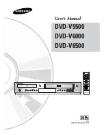
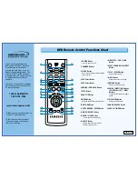
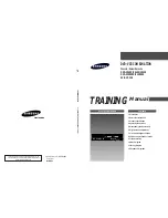
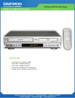
NTSC/PAL
PULL OPEN
DV- N C 1 0 0
OPERATE
OPEN/CLOSE
PLAY
STOP
DVD
VCR
CH
TIMER
REC
PLAY
REW
FF
STOP/
EJECT
(TRACKING)
OUTPUT
1st Edition
Summary of Contents for DV-NC100S
Page 48: ...1 12 3 1 12 4 H9740SCM1 Main 1 9 Schematic Diagram VCR Section ...
Page 50: ...Main 3 9 Schematic Diagram VCR Section 1 12 7 1 12 8 H9740SCM3 ...
Page 51: ...Main 4 9 Schematic Diagram VCR Section 1 12 9 1 12 10 H9740SCM4 ...
Page 52: ...1 12 11 1 12 12 H9740SCM5 Main 5 9 Schematic Diagram VCR Section ...
Page 53: ...Main 6 9 Schematic Diagram VCR Section 1 12 13 1 12 14 H9740SCM6 ...
Page 54: ...Main 7 9 DVD Open Close Schematic Diagrams VCR Section 1 12 15 1 12 16 H9740SCM7 ...
Page 55: ...Main 8 9 Schematic Diagram VCR Section 1 12 17 1 12 18 H9740SCM8 ...
Page 56: ...1 12 19 1 12 20 H9740SCM9 Main 9 9 Schematic Diagram VCR Section ...
Page 58: ...Jack A Schematic Diagram 1 12 23 1 12 24 H9740SCJ ...
Page 59: ...AFV Schematic Diagram 1 12 25 1 12 26 H9740SCAFV ...
Page 60: ...1 12 27 1 12 28 H9740SCD1 DVD Main 1 3 Schematic Diagram DVD Section ...
Page 61: ...1 12 29 1 12 30 H9740SCD2 DVD Main 2 3 Schematic Diagram DVD Section ...
Page 69: ...1 12 46 BE5900G04012 1 12 45 DVD MAIN CBA Top View ...
Page 70: ...1 12 47 1 12 48 BE5900G04012 DVD MAIN CBA Bottom View ...