background image

1

DV-L70U

SX9Q8DV-L70U/

SERVICE MANUAL

Page

1. IMPORTANT SAFEGUARDS AND PRECAUTIONS ...................................................................... 1-1
2. FEATURES/3. SPECIFICATIONS .................................................................................................. 2-1
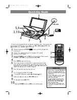
4. PART NAMES ................................................................................................................................. 4-1
5. DISASSEMBLY METHOD .............................................................................................................. 5-1
6. ADJUSTMENT METHOD ................................................................................................................ 6-1
7. TEST MODE ................................................................................................................................... 7-1
8. TROUBLESHOOTING .................................................................................................................... 8-1
9. IC FUNCTION LIST ......................................................................................................................... 9-1

10. SEMICONDUCTOR LEAD IDENTIFICATION .............................................................................. 10-1
11. WIRING DIAGRAM ....................................................................................................................... 11-1
12. BLOCK DIAGRAMS ...................................................................................................................... 12-1
13. SCHEMATIC DIAGRAMS ............................................................................................................. 13-1
14. PRINTED WIRING BOARD ASSEMBLIES ................................................................................... 14-1
15. REPLACEMENT PARTS LIST ...................................................................................................... 15-1
16. PACKING OF THE SET ................................................................................................................ 16-1

 CONTENTS

SHARP CORPORATION

In the interests of user-safety (Required by safety regula-
tions in some countries) the set should be restored to its
original condition and only parts identical to those specified
be used.

MODEL

DV-L70U

SERVICE MANUAL

PORTABLE DVD VIDEO PLAYER

MODEL DV-L70U

PORTABLE DVD VIDEO PLAYER

Summary of Contents for DV-L70U

Page 1: ...10 1 11 WIRING DIAGRAM 11 1 12 BLOCK DIAGRAMS 12 1 13 SCHEMATIC DIAGRAMS 13 1 14 PRINTED WIRING BOARD ASSEMBLIES 14 1 15 REPLACEMENT PARTS LIST 15 1 16 PACKING OF THE SET 16 1 CONTENTS SHARP CORPORATION In the interests of user safety Required by safety regula tions in some countries the set should be restored to its original condition and only parts identical to those specified be used MODEL DV L...

Page 2: ...o earth exposed metal part having a return path to the chassis metal cabinet screw heads knobs and control shafts etc and measure the AC voltage drop across the resistor Reverse the AC plug on the set and repeat AC voltage DVM AC SCALE 1 5k ohms 10W CONNECT TO KNOWN EARTH GROUND TO EXPOSED METAL PARTS 0 15 µF TEST PROBE measurements for each exposed part Any reading of 0 45V rms this corresponds t...

Page 3: ...DV L70U 1 2 ...

Page 4: ...he end of their useful life the Nickel Cadmium battery can be dropped off at the nearest collection center for recycling For information on the nearest collection center call 1 800 8 BATTERY or your local recycling center If you are located outside the United States contact your local authorities for information concerning proper disposal and or recycling of this battery SHARP s involvement in thi...

Page 5: ...ese jacks to connect to a TV for big screen viewing Output only is supported for S video An S video signal cannot be input to your DVD video player 1 Manufactured under license from Dolby Laboratories Dolby Pro Logic and the double D symbol are trademarks of Dolby Laboratories Confidential Unpulished Works C 1992 1997 Dolby Laboratories Inc All rights reserved 2 DTS and DTS Digital Surround are tr...

Page 6: ...ty DVD Operation 30VA Charging 100V 30VA Rated Output DVD Operation 9V DC Charging 9V DC Dimensions 58 W 104 D 275 H mm 219 64 47 64 1053 64 Weight 170g 0 38 lbs Battery Pack Specifications Type Lithium ion type DC output 7 4V Capacity 4200mAh Operating temperature 0 C to 40 C 32 F to 104 F charging 10 C to 30 C 50 F to 86 F Max Dimensions 184 W 134 5 D 14 5 H mm 71 4 519 64 37 64 without protrudi...

Page 7: ...DV L70U For details on the use of each control 4 PART NAMES 4 1 ...

Page 8: ...ctor 5 8 Remove the screws 6 fixing the DC jack PWB 9 Remove the four LCD rubber caps 7 10 Remove the four screws 8 Note Be careful not to forget to put space washers when assembling because they are tightened with the above screws 11 Remove the cabinet D At this time remove engagement claws two on the upper LCD panel two on the right and left sides two on the lower LCD panel Note Do not break the...

Page 9: ...Setting Monoscope full screen Adjustment Method Adjust the screen so that it is located in the center Adjustment VR R1104 Adjustment Point Observe the 3PIN of TP1191 with a frequency counter Input Signal Setting No input external input mode Adjustment Method Adjust it so as to get the HSY frequency of 15 735 0 01KHz 63 554µS HSY 15 735KHz 63 554µS 6 2 ADJUSTMENT PROCEDURE AND METHOD OF LCD PWB SID...

Page 10: ... key is pushed at the same time and made power source on 2 It moves to the special mode SP MODE and a BACKLIGHT HI LOW OFF key is pushed and turned off 3 After setting is completed a power source is turned off 4 Again a UP DOWN key is pushed at the same time and a power source is turned on and made special mode 5 An INPUT DVD key is pushed and it becomes adjustment mode 6 Each operation in the adj...

Page 11: ...justment Point Dual the oscilloscope to 3PIN VG and 5PIN VB and GND of TP1901 Input Signal Setting Black and white 10STEP Adjustment Method Adjust the white balance blue so that peak peak the equal of green and blue output become equal Adjustment VR SCOL Adjustment Point Connect the oscilloscope to 5PIN VB and GND of TP1901 Input Signal Setting 100 color bar Adjustment Method Adjust the blue ampli...

Page 12: ...nel as shown in the figure and check by shaking your head and seeing whether stripes appear If the adjustment is improper you will see stripes in the longitudinal direction Perform the adjustment so that they do not appear Type drawing Optimal point Adjust within the above range to fix the optimal point Direction of stripe Adjustment VR OSDH Adjustment Point Visual observation Adjustment method Ad...

Page 13: ...Adjustment VR GPOS Adjustment Point Comparison with the standard set Input Signal Setting 10STEP signal Check and Check whether the luminance and gradation of 10STEP signal are not different in comparison with the standard set If they are different adjust them so as to get equal to the standard set 3 Luminance gradation check 4 Depth check Adjustment VR S depth Adjustment Point Comparison with the...

Page 14: ... the remote controller is pushed The playback key of the remote controller is pushed The reactivation key of the remote controller is pushed The playback key of the remote controller is pushed Model name Model number DVL70U 00000701 Region No Region cord 1 00000001 Micro code is the thing of the process program of the system integrated circuit Color bar display 20000001 00000000 The preparation da...

Page 15: ...fset value 0 layer focus balance value The playback key of the remote controller is pushed DDT step 2 DD000202 0000 A track slead on are done after RF gain outline adjustment and track balance adjustment are done 0 layer RF gain value Track balance value 0 layer focus balance value The playback key of the remote controller is pushed DDT step 3 DD000203 0000 Just focus adjustment is done RF gain ad...

Page 16: ...W CHART NO 2 FLOW CHART NO 3 FLOW CHART NO 4 NO The key matrix circuit of IC3200 is checked 30 27pins S0 S3 26 20pins K0 K3 D3102 D3103 3108 Replace key switch Is key switch contact and installation state YES YES Check the main PWB unit of IC3200 and IC3205 Key manipulation on the LCD function side doesn t function FLOW CHART NO 5 When S1001 is pressed are the pins 1 and 2 short circuited NO NO YE...

Page 17: ...s pressed is the base of Q309 0 8V NO NO NO Is the voltage of 3 4V being applied to the emitter of Q308 NO Is the drive signal LDO2 of Q308 LD POWER CTL being output to the pin 4 of IC303 When S502 is pressed is the base of Q309 0 8V YES The CD disc is not recognized When the laser beam does not go on FLOW CHART NO 11 The DVD disc is not recognized When the laser beam does not go on FLOW CHART NO ...

Page 18: ... normal YES The outside output terminal J6002 peripheral is checked from 12 of IC2102 8 pin The VIDEO DRIVER circuit composed of Q2201 Q2206 is examined Picture do not operate normally FLOW CHART NO 14 Does 13 pin of IC1801 gain the control voltage about 3 1V of TINT YES YES NO Is the outside horizontal synchronizing of 34 pin of IC1801 normal NO NO Is the 14 16 pin of IC1801 doing oscillation 3 5...

Page 19: ...tted to 36 pin of IC1801 Is a synchronizing signal being outputted to 35 pin of IC1801 NO Check the betweenthe emmiter and pin 36 of IC1801 Check the pins 38 44 43 of IC1101 and pins L1109 D1105 IC1102 Q1101 etc Check the peripheral circuit pins 71 70 of IC1101 and R1103 image plane center position Is the horizontal position of the picture image normal YES The readjustment of R1103 PIC CENTER POS ...

Page 20: ...Digital circuit 23 Reset I Reset signal active LOW 24 PAL NTSC I NTSC PAL select This pin active only Reset time NTSC Low PAL High 25 32 DVIN7 0 I 8 bit Multiplexd Y Cr Cb 4 2 2 data ITU Rec656 input 1 or Multiplexd Y data ITU Rec656 601 input in 16 bit input mode DVIN7 MSB 33 TVIN I TEST data input 34 EXT I O Csync Frame sync output or external VBI information input 35 F Vsync I O Frame sync or V...

Page 21: ...27 RPP O RF ripple peak 28 RFO O Equalizing RF output 2 3 V 29 NC NC terminal To be connected to GND 30 NC NC terminal To be connected to GND 31 VccR Power terminal RF 32 DPDB I Pit depth adjustment VrD When D PDB is raised the A B side delay increases 33 TEB I TE balance VrD When TEB is raised the TP side gain increases and the A C side delay increases 34 FEB I FE balance VrD When FEB is raised t...

Page 22: ...D2 EQD NC Vcc2 PSC FEB TEB GND P2TP P2TN LDO2 MDI2 VrA VrD Vdd DPAC DPBD DPD1 DPD2 SCB SCL SCD VRCK 1 2 3 4 5 6 7 8 9 10 11 12 13 14 15 16 17 18 19 20 21 22 23 24 25 26 27 28 29 30 31 32 48 47 46 45 44 43 42 41 40 39 38 37 36 35 34 33 64 63 62 61 60 59 58 57 56 55 54 53 52 51 50 49 APC1 sel RF R gain Adjust EQ F gain Adjust F gain Adjust RF Ripple creation FE creation DPDTE creation FE gain Adjust...

Page 23: ...23 HA1 I MPU address bus TTL level 24 PLCK I O Read channel clock input output terminal 25 ED0 User use is prohibited N C since it is for shipping adjustment Open 26 ED1 27 ED2 28 ED3 29 ED4 30 ED5 31 ED6 32 ED7 33 TEST I For shipping adjustment Set to L 34 PDON O PLL phase error signal output Negative polarity 35 PDOP O PLL phase error signal output Positive polarity 36 RLLD O RLL detection resul...

Page 24: ...TL level 76 MD2 I O External RAM data bus TTL level 77 MD1 I O External RAM data bus TTL level 78 MD0 I O External RAM data bus TTL level 79 SD7 O MPEG data output 80 SD6 O MPEG data output 81 SD5 O MPEG data output 82 SD4 O MPEG data output 83 DVSS Digital power 0V For logic cell 84 DVDD3 Digital power 3 3V For logic cell 85 SD3 O MPEG data output 86 SD2 O MPEG data output 87 SD1 O MPEG data outp...

Page 25: ...power down state 480 ns is required to recover from the deep power down state If the RP pin becomes Low the whole chip operation is interrupted and reset After recovery the device is set to array read state 28 OE Input Output enable When OE is set to Low data is output from the DQ pin When OE is set to High the DQ pin is set to float state Write enable Command user interface data Q register and ad...

Page 26: ...O1 TIOCB3 P2 2 PO2 TIOCC3 P2 3 PO3 TIOCD3 P2 4 PO4 TIOCA4 P2 5 PO5 TIOCB4 P2 6 PO6 TIOCA5 P2 7 PO7 TIOCB5 P4 7 AN7 DA1 P4 6 AN6 DA0 P4 5 AN5 P4 4 AN4 P4 3 AN3 P4 2 AN2 P4 1 AN1 P4 0 AN0 V ref AV cc AV ss PA5 A21 IRQ5 PA4 A20 IRQ4 PA3 A19 PA2 A18 PA1 A17 PA0 A16 PB7 A15 PB6 A14 PB5 A13 PB4 A12 PB3 A11 PB2 A10 PB1 A9 PB0 A8 PC7 A7 PC6 A6 PC5 A5 PC4 A4 PC3 A3 PC2 A2 PC1 A1 PC0 A0 P35 SCK1 P34 SCK0 P3...

Page 27: ...ital GND 33 VDD Power 3 3V 34 EXPBU 0 In Output General use input output terminal Gr B 35 EXPBU 1 In Output General use input output terminal Gr B 36 EXPBU 2 In Output General use input output terminal Gr B 37 EXPBU 3 In Output General use input output terminal Gr B 38 EXPC 0 In Output General use input output terminal Gr C 39 EXPC 1 In Output General use input output terminal Gr C 40 EXPC 2 In Ou...

Page 28: ... 5 BUFDO BUFDI SBUFBO SBUFBI SBUFAO SBUFAI MRST MODE BUFCO TEST BUFCI VSS VDD SOUT 3 SOUT 4 SOUT 5 MRST MODE SEL TEST CK VSS VSS EXPD 2 EXPD 1 EXPD 0 EXPC 5 EXPC 4 EXPC 3 VSS EXPC 2 EXPC 1 EXPC 0 EXPBU 3 EXPBU 2 EXPBU 1 EXPBU 0 VDD VSS SOUT 2 SOUT 1 SOUT 0 S2 5 S2 4 S2 3 VSS S2 2 S2 1 S2 0 Q2 7 Q2 6 Q2 5 Q2 4 VDD VSS EXPBL 3 EXPBL 2 EXPBL 1 EXPBL 0 EXPAU 3 EXPAU 2 VDD VSS EXPAU 1 EXPAU 0 EXPAL 3 E...

Page 29: ...nnected to VDD it becomes the data line 15 12 of the 16 bit host 3 6 HD 15 12 3 S I O data bus When HWID is connected to GND it becomes CD DSP serial input port pin as specified below 6 CDDAT HD 12 I I CD DSP bit clock input 5 CDDAT HD 13 I I CD DSP data input 4 CDFRM HD 14 I I CD DSP LR clock frame input 3 CDERR HD 15 I I CD DSP data error input 22 HA 3 0 I I Host address input The address signal...

Page 30: ... The signal is used as the qualifier of the data and sync signal 90 HSYNC 3 S I O Horizontally sync bidirection signal pin The polarity and length are programmable 89 VSYNC 3 S I O Vertically sync bidirectional signal pin The polarity and length are programmable 91 FI 3 S I O Field identification bidirectional signal pin The polarity is programmable 88 CBLANK O O Composite blank output The wavefor...

Page 31: ... RAMDQM O O SDRAM data masking active high output 54 RAMCS0 O O SDRAM chip select active low output For lower order of 2Mbyte device 55 RAMCS1 O O SDRAM chip select active low output For higher order of 2Mbyte device 60 RAMWE O O SDRAM write enable active low output 127 SCNENBL I I Test pin Usually connected to GNG 83 TESTMODE I I Test pin Usually connected to VDD 139 ICEMODE I I Test pin Usually ...

Page 32: ...Input Output Mask Makes data output Hi Z tsHZ after the clock and masks the output Blocks data input when L U DQM active 2 3 5 DQ0 15 Data Input Output Data inputs outputs are multiplexed on the same pins 6 8 9 11 12 39 40 42 43 45 46 48 49 Vcc Vss Power Supply Ground Power and ground for the input buffers and the core logic 25 1 26 50 Vcc VssO Data Output Power Ground Isolated power supply and gr...

Page 33: ...t stop selection terminal 27 A11 Drive output 1 12 VPUMP Booster terminal 28 A12 Drive output 1 13 BC1 Booster capacitor connection terminal 29 NC N C 14 BC2 Booster capacitor connection terminal 30 PWMSW PWM frequency selection terminal 15 GND GND terminal 31 VM12 Motor power terminal 1 16 VDD Power terminal 32 VM11 Motor power terminal 1 9 14 11 10 8 9 30 0 1µF 0 1µF 100µF VPUMP BC1 BC2 VDD STAR...

Page 34: ... input terminal 8 REG_OUT Constant voltage output 20 VCC VCC collector of external Tr 21 GND GND 9 REG_B Connected to the base of external Tr 22 OUT3 CH3 negative output terminal 10 BIAS Bias input terminal 23 OUT3 CH3 positive output terminal 11 IN1 CH1 gain adjustment input terminal 24 OUT2 CH2 negative output terminal 12 IN1 CH1 gain fixed input terminal 25 OUT2 CH2 positive output terminal 9 1...

Page 35: ...tput terminal Usually fixed to L 20 P2VREF PLL system 2VREF terminal 21 SPDO O VCO center frequency shift terminal 22 PDOS O EFM and PLCK signal phase error signal output terminal To be used when x8 speed operation is used 23 PDO O EFM and PLCK signal phase error signal output terminal 24 XMAXS O TMAX detection result output terminal To be selected with command bit TMPS 25 TMAX O 26 LPFN I Reverse...

Page 36: ...zer from the IO0 1 terminal and to output the dual value PWM from disc equalizer of IO2 3 terminal L Active 64 CKSE X tal selection terminal When 16 9344 MHz H When 33 8688 MHz L 65 DACT Test terminal 66 TESIN Test input terminal 67 TESIO1 Test input output terminal 68 VSS Digital ground terminal 69 PXI DSP system clock oscillation circuit input terminal 70 PXO DSP system clock oscillation circuit...

Page 37: ...eed playback L H x4 speed playback L L x8 speed playback Block Diagram 76 DVDD 77 RO 78 DVSS 79 DVR 80 LO 81 DVDD 82 TEST1 83 TEST2 84 TEST3 85 BUS0 86 BUS1 87 BUS2 88 BUS3 89 VDD 90 VSS 91 BUCK 92 CCE 93 TEST4 94 TEMOD 95 RST 96 TEST0 97 HSO 98 UHSO 99 EMPH 100 LRCK 50 DMO 49 FVO 48 FMO 47 TEBC 46 RFGC 45 VREF 44 TRO 43 FOO 42 TEZI 41 TEIN 40 TSIN 39 SBAD 38 FEIN 37 RFRP 36 RFZI 35 RFCT 34 AVDD 3...

Page 38: ... reset state 1 23 CS IWO I Chip selection input format selection 2 24 MODE I Mode control selection H Software L Hardware 1 25 MUTE I Mute control 1 26 MD DM0 I Mode control data deemphasis selection 1 1 27 MC DM1 I Mode control BCK deemphasis selection 2 2 28 ML IIS I Mode control latch input format selection 1 Note 1 Pins 22 24 25 26 27 and 28 With Schmidt trigger input pull up resistor 2 Pin 23...

Page 39: ...30 HIM Input CPU bus control selection signal I M mode H L 31 MRST Input Reset signal 32 VSS Digital GND 33 VDD Digital power 3 3V 34 PXDO 0 Output Pixel data output 35 PXDO 1 Output 8 bit parallel video data conforming to ITU R BT 601 and BT 656 standard Cb Y Cr Y 36 PXDO 2 Output MSB PXDO 7 LSB PXDO 0 37 PXDO 3 Output 38 PXDO 4 Output 39 PXDO 5 Output 40 VSS Digital GND 41 VDD Digital power 3 3V...

Page 40: ...rce Dec NTSC Enc 3ch D A built in Edge creation SPT circuit Digital dinamic r circuit Digital color correction Color offset correction White correction DR SPT circuit 8 1 1 1 1 Pin No Terminal name I O Operation function 1 IN I Error amplifier inversion input terminal 2 SCP Capacitor connection terminal for soft start SCP setting 3 VCC Power terminal 4 BR CTL I Output current setting control termi...

Page 41: ...put 16 MDS Input for display mode setting 52 TEST Test setting input 17 GND Ground power terminal 53 MON_A Test setting output 18 EXCL Clock input output 54 MON_B Test setting output 19 GND Ground power terminal 55 MON_C Test setting output 20 MDW Input for display mode setting 56 MON_D Test setting output 21 MDN Input for display mode setting 57 CLS Clock signal output for gate driver 22 PWM Back...

Page 42: ...djustment can be done between black black of the RGB output signal the swing and the dynamic range ADJUST This terminal is preset inside 27 GAMMA 0 Adjustment can be done the point of the gamma 0 This terminal is preset inside 29 BRIGHT A gamma compensation curve and the adjustment of the swing of common output can be done 30 SUB BRIGHT B It interlocks with the gamma compensation curve and R and t...

Page 43: ...EG1 REG2 REG3 TRAP KILLER PICTURE BGP GEN Window Pulse GEN F F AGCAMP AGCDET SYNCSEP CLAMP VREF INV ϒ AMP MATRIX INT EXT SW ϒ AMP ϒ AMP INV INV Block Diagram Pin No Terminal name Operation function 47 AGC OUT It is the terminal which the voltage detected in the automatic gain control detector circuit of the luminance signal is outputted in Output voltage rises the output voltage 48 PICTURE The fre...

Page 44: ...om DVD system computer 8 O SOUT Serial data output To DVD system computer 9 I SIN Serial data input From DVD system computer 10 I SYNC Composite sync signal input From LCD decoder IC 11 I PLLD TVPLL lock signal input From TV tuner 12 O PLCS TVPLL load EN output To TV tuner 13 O PCLK Clock output for inner communication To TV tuner E2 PROM and DAC IC 14 O POUT Data output for inner communication To...

Page 45: ...C 52 O LED1 LED control green To LED lighting circuit 53 O AV S TD DVD video audio selection output To video SW IC audio SW IC 54 O LED2 LED control red To LED lighting circuit 55 O AV P TD DVD video audio selection output To video SW IC audio SW IC 56 O DEF Defeat output 57 O EPCS E2 PROM chip select To E2 PROM 58 O DACS DAC chip select To adjustment DAC IC 59 O FLOF Not used 60 O IN H External i...

Page 46: ...ut READY signal output during serial communication with DVD H Command reception disable BUSY state L Command reception enable READY state 18 O POW Power on off control DC DC power control H Power ON L Power OFF stand by 19 I PIN Data output for inner communication Serial data input to E2 PROM 20 O K3 Not used 22 O K2 Key matrix output2 23 25 O K1 Key matrix output1 26 O K0 Key matrix output0 27 I ...

Page 47: ...t H During data transmission to DAC L When data is not transmitted 59 O FLOF DVD video mute H Normal L DVD video mute 60 O IN H External input control H External input L DVD TV mode 61 I PSW Not used 62 O SMUTE Audio mute output L Speaker sound mute 63 H Normal 65 O PMUTE Video mute output L Video mute H Normal 79 O FMCS Not used Timer RAM 512byte ROM 32Kbyte It is interrupted CGRAM ADDRESS BUS DA...

Page 48: ... register is output 16 I Shift clock input terminal The input signal form the DI terminal is input into 12 bit shift register when the shift clock reises 15 I Load signal input terminal When H level is input the data of the 12 bit shift register is loaded to the decoder and register for D A output 18 O D A output teminal Analog data of 8 bit D A converter with OP amplifier is output 19 2 3 4 5 6 7...

Page 49: ...truction decode control clock generation Wave voltage detection Write inhibition High voltage generation bit EEPROM Aray 1 024 6bit 6bit 16bit 16bit 9 25 IC3205 S875045B Voltage detection circuit Phase fault protection circuit Delay circuit 1 4 2 3 5 VOUT VOR VIN VSS CD Voltage regulator Pin No Terminal name Remarks 1 VOUT Output terminal of voltage regulator 2 Vss GND terminal 3 CD External capac...

Page 50: ...SGND1 Signal ground1 9 OUT2A Output2 Positive 2 IN1 Input1 10 GND2 Power ground2 3 n c Not connected 11 n c Not connected 4 n c Not connected 12 OUT2B Output2 Negative 5 Vp Supply voltage 13 OUT1B CH2 gain fixed input terminal 6 IN2 Input2 14 GND1 CH3 gain adjustment input terminal 7 SGND2 Signal ground2 15 n c Not connected 8 n c Not connected 16 OUT1A VCC Block Diagram 16 OUT1A 13 14 5 OUT1B GND...

Page 51: ...scillator Vref 2 5V 16 15 9 1 2 7 10 8 11 6 3 4 5 12 14 13 Error Amp1 VCC 2 0V 1 4V 2 5V Vref 2 Vref Vref Vref Reference Voltage R U V L O R S Latch Output1 Output2 Error Amp2 PWM Comprator1 PWM Comprator2 GND Short Circuit Protection Comparator ...

Page 52: ...16GEZZ IC512 RH iX1535GEZZ IC602 RH iX0750TAZZ IC2102 VHiTK15400 1 IC3201 VHiMB8346BV 1 IC703 VHi10324AFV 1 IC506 RH iX1618GEZZ IC3202 VHiBR93L46F 1 IC1900 VHiBA7046F 1 LZ9GJ18 SHARP JAPAN Y Y WW XXX IR3Y298 SHARP JAPAN Y Y WW X IC1801 VHiiR3Y29BM 1 IC1902 VHiTC4S81F 1 IC1102 VHiNJM2107F 1 IC2103 VHiTC4S66F 1 IC3601 VHiTK11835 1 IC707 RH iX1473GEZZ X601 RCRSC0031GEZZ X702 RCRSC0035GEZZ IC6202 IC62...

Page 53: ...DV L70U 11 WIRING DIAGRAM 11 1 ...

Page 54: ...1 2 3 4 5 6 7 8 9 10 11 12 13 14 15 16 17 18 19 20 A B C D E F G H I J DV L70U DV L70U 12 1 12 2 12 BLOCK DIAGRAMS 12 1 MAIN BLOCK DIAGRAM ...

Page 55: ...1 2 3 4 5 6 7 8 9 10 11 12 13 14 15 16 17 18 19 20 A B C D E F G H I J DV L70U DV L70U 12 3 12 4 12 2 LCD BLOCK DIAGRAM ...

Page 56: ...1 2 3 4 5 6 7 8 9 10 11 12 13 14 15 16 17 18 19 20 A B C D E F G H I J DV L70U DV L70U 12 5 12 6 12 3 POWER BLOCK DIAGRAM ...

Page 57: ...1 2 3 4 5 6 7 8 9 10 11 12 13 14 15 16 17 18 19 20 A B C D E F G H I J DV L70U DV L70U 12 7 12 8 12 4 INVERTER BLOCK DIAGRAM ...

Page 58: ...1 2 3 4 5 6 7 8 9 10 11 12 13 14 15 16 17 18 19 20 A B C D E F G H I J DV L70U DV L70U 13 1 13 2 13 SCHEMATIC DIAGRAMS 13 1 MAIN 1 CIRCUIT SCHEMATIC DIAGRAM ...

Page 59: ...1 2 3 4 5 6 7 8 9 10 11 12 13 14 15 16 17 18 19 20 A B C D E F G H I J DV L70U DV L70U 13 3 13 4 13 2 MAIN 2 CIRCUIT SCHEMATIC DIAGRAM ...

Page 60: ...1 2 3 4 5 6 7 8 9 10 11 12 13 14 15 16 17 18 19 20 A B C D E F G H I J DV L70U DV L70U 13 5 13 6 13 3 MAIN 3 CIRCUIT SCHEMATIC DIAGRAM ...

Page 61: ...1 2 3 4 5 6 7 8 9 10 11 12 13 14 15 16 17 18 19 20 A B C D E F G H I J DV L70U DV L70U 13 7 13 8 13 4 LCD CIRCUIT SCHEMATIC DIAGRAM å AND SHADED COMPONENTS SAFETY RELATED PARTS å ...

Page 62: ...DV L70U 14 1 14 PRINTED WIRING BOARD ASSEMBLIES 14 1 MAIN PWB Componet Side A B C D E F G H I J 1 2 3 4 5 6 7 8 9 10 ...

Page 63: ...DV L70U 14 2 A B C D E F G H I J 1 2 3 4 5 6 7 8 9 10 Wiring Side ...

Page 64: ...1 2 3 4 5 6 7 8 9 10 11 12 13 14 15 16 17 18 19 20 A B C D E F G H I J DV L70U DV L70U 14 3 14 4 14 2 LCD OPERATE PWB LCD PWB Componet Side OPERATE PWB Componet Side Wiring Side Wiring Side ...

Page 65: ...DV L70U M E M O 14 5 ...

Page 66: ...E AB Q3102 VSDTA144EE 1 DTA144EE AA Q3103 VS2SC4738Y 1 2SC4738Y AA Q3201 VS2SC4738Y 1 2SC4738Y AA Q3202 VS2SC4738Y 1 2SC4738Y AA Q3203 VSDTA144EE 1 DTA144EE AA Q3204 VSDTA144EE 1 DTA144EE AA Q3601 VS2SA1362GR 1 2SA1362GR AC Q6000 VS2SD1306 E1E 2SD1306 AD Q6001 VS2SD1306 E1E 2SD1306 AD Q6002 VSDTA114EE 1 DTA114EE AB Q6612 VS2SC4213B 1 2SC4213B AC Q6613 VS2SC4213B 1 2SC4213B AC Q6615 VS2SC4213B 1 2S...

Page 67: ...CY1CB333K 0 033 16V Ceramic AA C409 VCKYCY1EB103K 0 01 25V Ceramic AA C410 VCCCCY1HH220J 22p 50V Ceramic AA C411 VCKYCY1AF105Z 1 10V Ceramic AC C412 VCKYCY1EB103K 0 01 25V Ceramic AA C413 VCKYCY1AF105Z 1 10V Ceramic AC C414 VCKYCY1EB103K 0 01 25V Ceramic AA C415 VCKYCY1HB471K 470p 50V Ceramic AA C416 VCKYCY1EB103K 0 01 25V Ceramic AA C417 VCKYCY1CB104K 0 1 16V Ceramic AB C418 VCKYCY1EB103K 0 01 25...

Page 68: ...amic AA C1815 VCKYCY1CF104Z 0 1 16V Ceramic AA C1816 VCKYCY1HF103Z 0 01 50V Ceramic AA C1817 VCCCCY1HH5R0C 5p 50V Ceramic AA C1818 VCKYCY1CF104Z 0 1 16V Ceramic AA 15 3 C420 VCKYCY1EB103K 0 01 25V Ceramic AA C421 VCKYCY1EB103K 0 01 25V Ceramic AA C424 VCCCCY1HH101J 100p 50V Ceramic AA C426 VCKYCY1CB104K 0 1 16V Ceramic AB C427 VCKYCY1EB103K 0 01 25V Ceramic AA C428 VCKYCY1EB103K 0 01 25V Ceramic A...

Page 69: ...1 50V Ceramic AA C3123 VCKYCY1HF103Z 0 01 50V Ceramic AA DUNTK5869KE52 MAIN PWB UNIT Continued C3124 VCSATE1AJ476M 47 10V Tantalum AD C3125 VCKYCY1AF105Z 1 10V Ceramic AC C3126 VCCCCY1HH470J 47p 50V Ceramic AA C3129 VCCCCY1HH471J 470p 50V Ceramic AA C3130 VCKYCY1HF103Z 0 01 50V Ceramic AA C3131 VCKYCY1CF104Z 0 1 16V Ceramic AA C3132 VCCCCY1HH471J 470p 50V Ceramic AA C3133 VCCCCY1HH471J 470p 50V Ce...

Page 70: ... AA R670 VRS TV1JD100J 10 1 16W Metal Oxide AA R701 VRS TW2ED1R0J 1 1 4W Metal Oxide AB R702 VRS TW2ED1R0J 1 1 4W Metal Oxide AB R703 VRS CY1JF151J 150 1 16W Metal Oxide AA R207 VRS CY1JF681J 680 1 16W Metal Oxide AA R208 VRS CY1JF391J 390 1 16W Metal Oxide AA R211 VRS CY1JF391J 390 1 16W Metal Oxide AA R212 VRS CY1JF103J 10k 1 16W Metal Oxide AA R215 VRS CY1JF201F 200 1 16W Metal Oxide AA R217 VR...

Page 71: ...A DUNTK5869KE52 MAIN PWB UNIT Continued R1803 VRS CY1JF102J 1k 1 16W Metal Oxide AA R1805 VRS CY1JF102J 1k 1 16W Metal Oxide AA R1806 VRS CY1JF391J 390 1 16W Metal Oxide AA R1807 VRS CY1JF333J 33k 1 16W Metal Oxide AA R1809 VRS CY1JF104J 100k 1 16W Metal Oxide AA R1810 VRS CY1JF183J 18k 1 16W Metal Oxide AA R1811 VRS CY1JF333J 33k 1 16W Metal Oxide AA R1812 VRS CY1JF683J 68k 1 16W Metal Oxide AA R...

Page 72: ...A R3219 VRS CY1JF104J 100k 1 16W Metal Oxide AA DUNTK5869KE52 MAIN PWB UNIT Continued R3220 VRS CY1JF473J 47k 1 16W Metal Oxide AA R3221 VRS CY1JF473J 47k 1 16W Metal Oxide AA R3222 VRS CY1JF561J 560 1 16W Metal Oxide AA R3223 VRS CY1JF102J 1k 1 16W Metal Oxide AA R3231 VRS CY1JF103J 10k 1 16W Metal Oxide AA R3232 VRS CY1JF103J 10k 1 16W Metal Oxide AA R3233 VRS CY1JF103J 10k 1 16W Metal Oxide AA ...

Page 73: ...S1001 QSW M0024TAZZ Switch Tray AE W3361 RRMCU0012TAZZ Remote Receiver AL DUNTK5870KE52 LCD PWB UNIT INTEGRATED CIRCUITS IC1000 VHiMB3800PV 1 MB3800PV AL IC1101 VHiLZ9GJ18 1 LZ9GJ18 AQ 15 8 IC1102 VHiNJM2107F 1 NJM2107F AE IC1103 VHiNJM4560M 1 NJM4560M AG TRANSISTORS Q1100 VS2SD999LK 1 2SD999LK AC Q1101 VS2SC4738Y 1 2SC4738Y AA Q1102 VS2SC2411KR 1 2SC2411KR AC Q1103 VS2SA1036KR 1 2SA1036KR AC DIOD...

Page 74: ...ch Enter AC DUNTK5870KE52 LCD PWB UNIT Continued C1140 VCKYCY1CF104Z 0 1 16V Ceramic AA C1141 VCKYCY1CF104Z 0 1 16V Ceramic AA C1142 VCKYCY1AF105Z 1 10V Ceramic AC C1143 VCCCCY1HH330J 33p 50V Ceramic AA C1144 VCCCCY1HH330J 33p 50V Ceramic AA C1145 VCKYCY1HB102K 1000p 50V Ceramic AA C1146 VCKYCY1CF104Z 0 1 16V Ceramic AA C1147 VCKYCY1HB561K 560p 50V Ceramic AA C1148 VCKYCY1CF104Z 0 1 16V Ceramic AA...

Page 75: ...Power FFC AE 31 QCNW 8099GEZZ Operation FFC AF 33 CCNW 8096GE01 LCD MAIN Harness AQ 33 1 QCNW 8096GEZZ Connecting Cord AK 33 2 QCNW 8098GEZZ Connecting Cord AK 33 3 MHNG 1071GEZZ Hinge R AG 34 QCNW 8161GEZZ Harness for LCD Frame AC Earth 35 QCNW 8097GEZZ Spindle Motor FFC AE 36 QCNW 8117GEZZ Inverter FFC AF 37 RSP Z0005GEZZ Speaker AP 38 RLCDT0001GEZZ LCD Panel CS 39 XWHJZ21 02040 Washer AA 40 XWH...

Page 76: ...15 15 5 16 17 1 2 2 10 6 11 7 1 8 Notes 1 When soldering the sled lead wire y it must be made in a soldering iron tip temperature of 290 20 C and within 3 seconds 2 Press fit dimension of motor pinion t When replacement or a djustment of the parts in this frame is necessary replace or adjust the mechanism ass y adjustment of the parts is completed 5 8 0 1 ...

Page 77: ...TGAN 3207GEZZ Guarantee Card TiNS 3698GEZZ Operation Manual SSAKA0100TAZZ Polystylene Bag Accessories SPAKF0195GEZZ Packing Meterial UBATU0241GEZZ Battery UADP 0194GEZZ AC Adapter QACCD3062GEZZ AC Power Cord QCNW 8340GEZZ S Video Video Cord QCNW 8341GEZZ Audio Cord RRMCG1223GESA Remote Control Unit SSAKA0096CEZZ Polystylene Sack å å Not Replacement Items ...

Page 78: ...ochigi 329 2193 Japan COPYRIGHT C 1999 BY SHARP CORPORATION ALL RIGHTS RESERVED No part of this publication may be reproduced stored in a retrieval system or transmitted in any form or by any means electronic mechanical photocopying recording or otherwise without prior written permission of the publisher TQ0766 S Dec 1999 Printed in JAPAN SA NS DV L70U ...

Page 79: ... VIEW A B C D E F G H 1 2 3 4 5 6 15 12 17 20 39 40 37 20 38 34 12 37 20 39 40 17 20 27 20 13 14 20 20 11 28 36 33 16 21 21 21 21 21 21 23 22 6 24 20 26 31 30 25 8 35 5 12 4 12 2 12 7 12 3 12 5 12 6 12 6 7 4 7 5 7 7 7 6 7 2 7 3 1 4 1 5 6 2 6 4 6 3 6 5 6 6 6 6 11 2 33 3 33 2 33 1 7 1 4 3 29 2 ...

Reviews: