DV-HR300U
SX3L5DV-HR300
SERVICE MANUAL
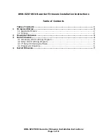
CONTENTS
In the interests of user-safety (Required by safety regulations
in some countries) the set should be restored to its original
condition and only parts identical to those specified be used.
MODEL
DV-HR300U
DVD VIDEO RECORDER
This document has been published to be used for
after sales service only.
The contents are subject to change without notice.
SHARP CORPORATION
Page
1. IMPORTANT SERVICE NOTES ........................................................................................................ 2
2. FEATURES ........................................................................................................................................ 6
3. SPECIFICATIONS ............................................................................................................................. 7
4. PART NAMES .................................................................................................................................... 9
5. DISASSEMBLY METHOD ............................................................................................................... 11
6. TROUBLESHOOTING ..................................................................................................................... 15
7. BLOCK DIAGRAMS ......................................................................................................................... 26
8. SCHEMATIC DIAGRAMS ................................................................................................................ 34
9. PRINTED WIRING BOARD ASSEMBLIES ..................................................................................... 60
10. REPLACEMENT PARTS LIST / EXPLODED VIEWS ..................................................................... 75
11. PACKING OF THE SET ................................................................................................................... 95
Summary of Contents for DV-HR300U
Page 25: ...25 DV HR300U M E M O ...
Page 26: ...26 27 DV HR300U DV HR300U 7 BLOCK DIAGRAMS 7 1 MAIN BLOCK DIAGRAM ...
Page 27: ...28 29 DV HR300U DV HR300U 7 2 SUB BLOCK DIAGRAM ...
Page 28: ...30 31 DV HR300U DV HR300U 7 3 POWER BLOCK DIAGRAM ...
Page 29: ...32 33 DV HR300U DV HR300U 7 4 DV BLOCK DIAGRAM ...
Page 48: ...68 DV HR300U A B C D E F G H I J 1 2 3 4 5 6 7 8 9 10 SIDE B SIDE A OPERATION R PWB ...
Page 49: ...69 DV HR300U A B C D E F G H I J 1 2 3 4 5 6 7 8 9 10 SIDE B SIDE A OPERATION L PWB ...
Page 50: ...70 DV HR300U A B C D E F G H I J 1 2 3 4 5 6 7 8 9 10 POWER PWB SIDE A ...
Page 51: ...71 DV HR300U A B C D E F G H I J 1 2 3 4 5 6 7 8 9 10 SIDE B ...
Page 52: ...72 DV HR300U A B C D E F G H I J 1 2 3 4 5 6 7 8 9 10 UV PWB SIDE A ...
Page 53: ...73 DV HR300U A B C D E F G H I J 1 2 3 4 5 6 7 8 9 10 SIDE B ...
Page 54: ...74 DV HR300U A B C D E F G H I J 1 2 3 4 5 6 7 8 9 10 LCD PWB SIDE A SIDE B ...