background image

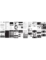
Summary of Contents for CE-121

Page 1: ...tions 2 2 Block diagram 4 3 LSI signal description 12 4 About servicing 17 5 Cassette operation 18 6 Check program 25 7 Circuit diagram 26 8 PC 1211 parts list guide 32 9 CE 121 parts list guide 34 MODEL PC 1211 CE 121 SHARP SERVICE MANUAL ...

Page 2: ...igits of exponent According to mathematical formula with priority consideration and judge function Program memory 1424 steps max PC1211 Data memory Fixed memory 26 memories Flexible memory commonly usable with the programmemory 178 memories max PC1211 Reserveprogram 18 kinds 48 steps max Input buffer 80 steps Data buffer 8 stages Functional buffer 16 stages but 15 stagesfor parenthesis Subroutine ...

Page 3: ...mory Physical dimensions 175 W x 70 D x 44 H mm 1 7 Others Four MR44 mercury batteries 300 hours 0 01 iw About 6 minutes Battery Battery life Power consumption Automatic power shut off 1 6 Power source 1 5 Programming language BASIC Beginner s All purpose Symbolic Instruction Code right left INS DEL down t up Cursor shift Insertion Deletion Line control 1 4 Editorial functions ...

Page 4: ... rn Z i 11 i CJ I 0 i r 00 0 A f c ___ I _ _ ___ I __ 0 a i VH q N l lt x 8V V 0 0 cc 0 u x I I 0 0 II l I u 0 il tOia OJG rn I c l 6 0 rn er s G 7 rn rn o rn rn rn c U l qs 00 v Cl rn CJ c I O llO u t i Cl ID c L lCJ __ J L lZO 0 u u Ul I s sc I en I z cc 0 in o E a CJ c 0 0 J m en CJ z 0 0 u l l z CJ z CJ l z CJ ...

Page 5: ...rforms some kinds of auxiliary CPUwhen looked in the viewthat it does not perform any decision by itself Clock stop Clock stop control I Power shut off control I Power off Display processingroutine Input buffer Computational result Error Arithmetic routine Character generator Cassette routine Print routine Buzzer Recognition of printer Key input routine Acknowledgement of the remaining program One...

Page 6: ... instruction code display at this case is transfered to the CPUII via the transfer buffer As the CPUII receivesthis instruction the CPUII then decodes this instruction display at this case and executes display processing Upon the completion of this processing it is then notified to the CPUI then the CPUI confirms the comple tion of the task by the CPUII before terminating their jobs CPU Il Ex Acti...

Page 7: ...1536 1472 1504 001 048 PC1211 Reserveprogram Program or flexible memory Fixed memories W Z Subroutine I FOR NEXT stack statement stack A certain number of C MOS RAM 1 3 chips 4K bits each and another RAM incorporated inside the display chip are used in this pocket computer having varieties of configurations as described below Map of 4K bit RAM 1536 Bytes 2 2 RAM en nd e II he le ...

Page 8: ...ytes 1 memory equivalent of the display chip 1 is used as a transfer buffer which is used in the transaction of instruction between the CPU I and the CPUII 16 bits 1 4bit 1 memory Fixed memory The total memory of 176 bytes from the display chip 2 and 3 is used as a fixed memories A V 22 memories 8 digitdisplaybuffer 40 bytes of 8 digit display buffer is used as a display data buffer during display...

Page 9: ...ss 00010001 S40 S32 S33 S34 Sl6 Sl7 Sl8 1 S2 A5 0 A5 1 DI04 DI02 DI04 DI02 Address 0 1 0 0 0 F 0 1 0 0 1 F 0 1 0 1 0 F Al I A8 A7 A6 A4 Hl DDD D H2 oo o H3 o o o H4 oo o H5 H6 ooo o H7 ooo o Sl S2 S3 S4 S5 Ex Displaying numerical figure 4 There are 8 x 40 320 bits 40 bytes of area in the display buffer in the display chip Display buffer XOOl 0100 H8 H7 H6 H5 H4 H3 H2 Hl XOOl 1000 Counter decoder H...

Page 10: ...al processing of display operation is indicated RAM data designatedby Hl H8 is sent out on SI S40 The data stored in the display buffer is carried through SI S40 Fig 2 3 2 to be fed to the LCD To indicate 4 on the display H4 and HS are engaged for SI H3 and HS for S2 etc all the same throughout S6 S40 Fig 2 3 2 S2 Sl H7 H6 LJl ____flJ L I H5 LJ H4 H3 H2 Hl GND VA Vs Vn1SP HA DI SP 0 5ms ...

Page 11: ...d from the LSI VA VM VB NOTE ata o The liquid crystal reference voltage VDISP is generated in the above circuitry in order to avoid occurrence of such unpleasant phenomena as blurred character or contrast variation that might degrade display performance which is caused by a slight voltage variation in the liquid crystal reference voltage VDISP since the 5 x 7 dot matrix liquid crystal is used in t...

Page 12: ...t RAMData Read Writesignal During display High ________ Depression of the key causesit momentary low 13 DIOl In Out Data Bus for address designation of the input buffer and 14 DI02 In Out transfer buffer in RAMand display chip 1 15 DI03 In Out During display High _ _ _ _ _ _ _ 16 DI03 In Out During read in Low 17 B8a Out AddressBus for address designation of the input buffer and 18 B7a Out transfe...

Page 13: ... Basicclock Pulse signalin 256KHz 11 RESET In All reset switch input 3 2 SC43178 CPU II Pin No Signalname In Out Description 41 Sn Out Key Strobe signal RAMAddresssignal 42 Si Out Key Strobe signal RAMAddresssignal 43 Sl3 Out Key Strobe signal 44 Sl2 Out 45 Sll Out During display High 46 SlO Out Depression of the key causesit momentary low 47 S9 Out 48 S8 Out 49 S7 Out 50 S6 Out 51 SS Out 52 S4 Ou...

Page 14: ...Display signal Common signalcounting pulse ruu Being generated during displaying 10 Smst 26 DISP Out Display command signal During display High Duringexecution Low 27 VM In LCDdisplay voltage Intermediate voltage of the segment signal 28 VA In LCDdisplay voltage High sidevoltage of the segment signal 29 GND In Supply voltage OV 30 H4 Out LCDcommon signals backplate 31 H7 Out 32 H3 Out 33 H6 Out 34...

Page 15: ...l Out For symbol display SHIFT DGE RAD GRAD RESERVE PRO RUN Same waveformas the segment signal 55 Kil In CPU I Busy signal High during the execution in CPUI Sl6a 56 K i2 In Expansion signal To be connected to Sl 2 CPUII for PC 1211 57 K i3 In Printer Busy signal Low when the priner is not operated 58 K i4 In Printer connection identifying signal Low when the printer is not connected 59 l 5 In Cass...

Page 16: ...15 CIN IN ouT OUf IN 13 1 2 1 5 2 CIN 12 4 IN ouT our IN 3 3 4 6 11 5 CIN 8 IN ouT OUT IN 9 6 10 12 7 CJN 11 IN our OUT IN 10 9 7 GND 5 4 2 6 3 2 5 4 3 7 GND 6 8 8 Vnn 14 13 12 11 10 9 Vno 14 13 12 11 10 9 TC4069P HEX inverter TC4011UBP Quad 2 input positive NAND gate 3 3 IC ...

Page 17: ...oard has to be bent in right angle after removing the screws d and e Inspection of the CPU I is possibleif the buzzer is removed after removing the screw c 4 The key printed board can be dismounted from the upper cabinet when the 9 screws f and 2 screws g are removed But care must be exercised in dismounting the printed board as key tops may come falling down one after another Replacement of the L...

Page 18: ...iod of about 6 seconds in order to avoid non recordable area located at the top of the tape and is also used for the cueing of the recordinghead 6 With this program or reserveprogram name is indicated 7 File name 8 Data memory is indicated with this code 9 Area for one data memory Recording method Data O and l are identified by changingthe frequency of the recording signal F4 Data memory recording...

Page 19: ...lse of 4KHz is output during that period Whenrecording signal O is to be recorded SI 5 is turned high level and the F4 output is inhibited during that period at which duration the reversesignal of HA clock pulse of 2KHz is carried on the recording signal Then this signalis supplied to the MIC terminal of the tape recorder via the modulation circuit of the CE121 Signalwaveform at the time of record...

Page 20: ... CR at the fallingedge of the input signal and B outputs a pulse which is dependable on the time constant of CR at the risingedge of the input signal The relay operates ON and OFF accordingto the current flow to the coil and it is activated when A is active and deactivated when B is active NR 5711 5 ru_ I L 0 04 7PF 470Kn 100 2 Kn 4 Ain Q 6 2SA733 MT A REMOTO 5 Bin QA 7 74 W Sl4 TC4528BP 33n 3 0 0...

Page 21: ... Make the RESERVE symbol indicated on the display after d1f essinf the IE TER key 2 NEW NEW_ RESERVE 3 IENTERI RESERVE 4 lSHFTI z Z _ RESERVE 5 P lSHFTlf Af lSHF rj A 204 Z P YA A 204 RESERVE 6 ENTER Z PRINT fAf A 204 RESERVE 7 lsHFTI X X _ RESERVE 8 1 SHFTlfAY lSHFTl A 76 X I YAT A 204 _ RESERVE 9 ENTER X INPUT JAY A 204 RESERVE 10 I SHFTI ISP CI RESERVE 11 A 76 A 204 RESERVE 12 IENTERI A 204 13 ...

Page 22: ... Step 16 repeat operation from Step 10 If the specific indication does not appear on the display repeat the procedure from Step 5 after entering A 204 100 If the specific indication is not to appear on the display even after this it requires detailed inspection No Read in Display Remarks 5 RUN Make sureof the tape recording location 6 RUN Depress the REC and PLAY buttons Then the cassette will com...

Page 23: ...e cassette tape comes to halt with indicated on the display 7 RUN 0 0 Return the tape to the beginning of the recording 8 RUN 0 0 0 0 9 CLO lsHFTI A CLO YA_ RUN 0 0 0 0 10 jENTERj RUN 0 0 0 0 The display con tents comes to dis appear from the display and the cassette tape starts to run generating the reproducing sound 11 RUN 0 0 0 0 Sound generation is interrupted and the cassette tape comes to ha...

Page 24: ...Recording sound goes out and 1O is displayed on the display for a period of about 1 second 4 RUN Cautions 1 Check the machine with the check procedure provided separately if the cassette tape happens to keep running at Step 3 the cassette tape fails to run at Step 5 or the cassette tape fails to stop at Step 6 2 Check the recording circuit of the CE121 if no recording sound is audible at Step 5 3 ...

Page 25: ...I SHFTI w s ISHFTI w ENTER 2 z p R I N T s I I I 8 3 B E E p 2 IENTERI 3 B E E P 2 IMODEI I 9 I G R A D iENTERl I 10 I l 11 I SHFTI ISPCI 0 I 4 7 IENTERI 0 l 4 7 IMODEI I 12 ISHFTI z I 13 s 14 IMODEI lsHFTllsPcl 0 I 4 7 15 RAD IENTERI I I 6 R lENTERl 0 K 1 I ENTERI T 17 s I 18 IENTERI I I r T r OFFI I 19 T I I 20 r r 21 I 22 23 I 24 25 26 I T l 27 I 28 I I I 29 30 I 31 I I I 32 33 I I l l l 34 I I...

Page 26: ...1I22 I23 I 24 SHFT DEG PRO Smm PLA REC STOP REMJT RAD GRAD DEF RUN I 0 0 I 5 5 5 5 5 5 5 5 5 E 0 1 0 0 I 0 0 K f 0 0 0 I 0 0 0 T s T I 0 I 0 0 0 0 I 0 0 0 0 0 0 0 I 0 0 0 0 0 0 0 0 I I 0 0 0 0 0 0 I 0 0 0 I I I I I I I I I I I I I I I I I I I I I I I I I I I I I HECK PROGRAM ...

Page 27: ...A_2 __ J __ lrt i ill 1 I I I 5 I I Bla I I T Q A l r i r tt t D 101 I 7 I Q _J ioxo r 3 1 1 CMT lOKn ___ lt t t t l 1 LJJ k 1 e Recording TC4011 UBP _ Signe q rc4 059 p l 12 I I IA3 514 REM OTO Signet I I I VGG I Op tion Jo Control I I 51 3 I l I DATAI 515 I I I cMT I I Ki4 C _l _ CCZZ J I Opt ion I 0 connect signal I 7 1 Operation Circuit Diagram 7 CIRCUIT DIAGRAM PARTS ...

Page 28: ... gi 0 TC4066P 113 I lM I I I I RAM A7 TC 5514PX 3 12 I I ___ I ___ I IA6 3 111 150Kn I L F4a1 GKD Tbermi stor I h tJ GND I I VA_ IA5 10l R I H I ___ VM r J TC4019P IJ i OWV I z IOOKn _ JOQµF IA4 Vg i lf 13 I 21 I i 2 Kn I I F3a 1 Vmsr Von _ I J 1 IA3 12 I L I VGG I I I A2 A7 GND A6 AB 111 I A5 Si r I A4 Sn I Al DIOl I A2 I DI02 A3 DI03 I F2a1 Al DI04 vGG RA 10 I I IOOKn _J 1 PF r n PWB ...

Page 29: ......

Page 30: ......

Page 31: ...0 28 FUNCTION 7 3 Key Circuit ...

Page 32: ... D 0 0000 o o o o o o ODD D D 0 D D D D D D O D DD D DODOO D 0 DODD D 0 DODOO DODOO 0 D DODO 0 0 D DODO D D D 0 0 D 0 D 0 0 DODO D 0 00000 DODOO D D D D 0 D D DODOO 0 ODDO D D 0 0 DD ODD OD D DO D D D 0 DODOO 0 0 DD OD ODDO 0 0 0 0 DODO 0 0 0 DOD 0 0 0 0 D D 0 ODO 0 D D D DOD D D 0 0 DODOO D D DOD D D 0000 ODD D D D O 0 D D 0 D 0 ODO 0000 D 0 D D ODD O D D D 0000 D D D D D D D DD OD OD DO 0 0 0 D ...

Page 33: ..._____ MSM401 3RS i ...

Page 34: ......

Page 35: ... 3 50WV 0 047 FF 470Kn VGG lOOKn e 16WV 15 14 Ef lO lF QB 2 SA733 12 10 GND BQB 9 W 11 TC4528 13 BP 33 1 50WV 0 047 lF 470 Kn lOOKn TC4069P DS1588Ll 6 DS1588Ll lOOKn 0 25 470Kn 2SA 733 CMT LOAD output KI 5 RECORD input F4 7 5 CE 121 Circuit Diagram ...

Page 36: ...RE YOTE EAR PHONE MIC I 3 L J 1 4 1 1 AAX3 W 33 n 1 Y4W 33 n NR 5711 r 5 I I 2 SC458KS 12 O OlµF 2SC458KS 25WV lOOK n 0 047J1 F 50WV t I i uo 2 SA 733 ...

Page 37: ......

Page 38: ...16 PGUM5 I I 90CCZZ Rubber connector c A F 17 VVLLF8017 JE I LCD N B B A 18 PTPEHl033CCZZ Tape for LCD c A A 19 LANGK1290CCZZ Angle for LCD c A D 20 PFiLWl230CCZZ Filter c A H 21 HDECAl527CCZZ Display mask c A c 22 PFiLWl228CCZZ Display filter c A c 23 PGUMMl254CCZZ Key rubber B A K 24 M5PRCI098CCZZ Earth spring c A A 25 JKNBZ1515CC04 Key top 18key N c A F 26 JKNBZl515CC05 Keytop 17key N c A F 27 ...

Page 39: ...I N 8 8 D VH i TC40 I I UBP I i C 8 A F VHiTC4019P I i C B A K VHiTC4066P I i C 8 A K VHiTC4069P I i C B A H VHiTC5514P I L S i RAM 8 B D VRC MT2BGl65J Resistor 1 BW 1 6Mohm 5 c A 8 VRD ST2BYIOIJ Resistor 1 BW 100ohm 5 c A A VRD ST2BY223J Resistor 1 BW 22Kohm 5 c A A VRD ST2BYl03J Resistor 1 BW 10Kohm 5 c A A VRD ST2BY104J Resistor 1 BW 100Kohm 5 c A A VRD ST2BYl05J Resistor 1 BW 1Mohm 5 I c A A V...

Page 40: ...33 l iii ...

Page 41: ...n N D A E VCEAAUICWI06Q Capacitor 10µF 16V c A B VCQYKUIHM472K Capacitor 0 0047µF 50V c A B VCQYKUIHM473K Capacitor 0 047µF 50V c A B VCTYPUIEXI03M Capacitor 0 01µF 25V c A B VCTYPUINXI04M Capacitor 0 1µF 12V c A B VHDDSl588Ll I Diode DS1588L1 B A B VH i NR57 I I 1 Relay NR5711 N B A w VHiTC4069P I I C TC4069P B A H VHiTC4528BP I I C TC4528BP N B A p VRD ST2BYI03 J Resistor 1 8W 10Kohm 5 c A A VRD...

Page 42: ...35 10 5 7 4 ...
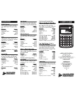
Page 43: ...SHARP CORPORATION Industrial Instruments Group Reliability Quality Control Department Yamatokoriyama Nara 639 11 Japan 1 981 March Printed in Japan ...

Reviews: