background image

– 1 –

CD-PC1881V

No. S0961CDPC1881

CD-PC1881V

• In the interests of user-safety the set should be restored to its

original condition and only parts identical to those specified be
used.

SERVICE MANUAL

This document has been published to be used
for after sales service only.
The contents are subject to change without notice.

SHARP CORPORATION

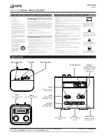
CD-PC1881V Video CD Mini System consisting of CD-PC1881V
(main unit), CP-C881 (front speakers), CP-SW881 (sub woofer),
GBOXS0026AWM1 (center speaker) and GBOXS0027AWM1
(surround speakers).

 CONTENTS

Page

SAFETY PRECAUTION FOR SERVICE MANUAL ...........................................................................................................  2
VOLTAGE SELECTION .....................................................................................................................................................  2
AC POWER SUPPLY CORD AND AC PLUG ADAPTOR .................................................................................................  2
SPECIFICATIONS .............................................................................................................................................................. 3
NAMES OF PARTS ...........................................................................................................................................................  4
OPERATION MANUAL ......................................................................................................................................................  7
DISASSEMBLY ..................................................................................................................................................................  8
REMOVING AND REINSTALLING THE MAIN PARTS ...................................................................................................  11
ADJUSTMENT .................................................................................................................................................................  12
BLOCK DIAGRAM ...........................................................................................................................................................  15
SCHEMATIC DIAGRAM ..................................................................................................................................................  18
VOLTAGE ........................................................................................................................................................................  30
WIRING SIDE OF P.W.BOARD .......................................................................................................................................  31
NOTES ON SCHEMATIC DIAGRAM ..............................................................................................................................  38
TYPES OF TRANSISTOR AND LED ...............................................................................................................................  38
WAVEFORMS OF CD CIRCUIT ......................................................................................................................................  39
TROUBLESHOOTING (CD SECTION) ...........................................................................................................................  40
FUNCTION TABLE OF IC ................................................................................................................................................  44
FL SEGMENT ................................................................................................................................................................... 56
PARTS GUIDE/EXPLODED VIEW

NTSC/PAL

Manufactured under license from Dolby Laboratories Licensing
Corporation.
DOLBY, the double-D symbol 

 and “PRO LOGIC” are

trademarks of Dolby Laboratories Licensing Corporation.

Summary of Contents for CD-PC1881V

Page 1: ...rround speakers CONTENTS Page SAFETY PRECAUTION FOR SERVICE MANUAL 2 VOLTAGE SELECTION 2 AC POWER SUPPLY CORD AND AC PLUG ADAPTOR 2 SPECIFICATIONS 3 NAMES OF PARTS 4 OPERATION MANUAL 7 DISASSEMBLY 8 REMOVING AND REINSTALLING THE MAIN PARTS 11 ADJUSTMENT 12 BLOCK DIAGRAM 15 SCHEMATIC DIAGRAM 18 VOLTAGE 30 WIRING SIDE OF P W BOARD 31 NOTES ON SCHEMATIC DIAGRAM 38 TYPES OF TRANSISTOR AND LED 38 WAVEF...

Page 2: ...age figure is displayed in the window next the adjustment screw QACCA0001AW00 Figure 2 AC POWER SUPPLY CORD AND AC PLUG ADAPTOR QACCB0006AW00 QACCE0008AW00 QACCJ0003AW00 QACCL0005AW00 This Video CD Mini System is classified as a CLASS 1 LASER product The CLASS 1 LASER PRODUCT label is located on the rear cover Use of controls adjustments or performance of procedures other than those specified here...

Page 3: ...Non contact 3 beam semi conductor laser pickup D A converter 1 bit D A converter Frequency Frequency response 20 20 000 Hz Dynamic range 90 dB 1 kHz Video CD section Video output format PAL PAL60 NTSC Tuner section Frequency range FM 88 108 MHz AM 531 1 602 kHz Cassette deck section Frequency response 50 14 000 Hz Normal tape Signal noise ratio 55 dB TAPE 1 playback 50 dB TAPE 2 recording playback...

Page 4: ...ton 24 VCD Skip Next Button CD Track Up Cue Button TUNER Preset Up Button TAPE 2 Fast Forward Button 25 Bypass Button 26 Normal Button 27 Timer Sleep Button 28 Clock Button 29 VCD Playback Control Auto Off Button 30 VCD CD Audio Mode Button 31 VCD On Screen Display On Off Button 32 On Stand by Button 33 Equalizer Mode Selector Button 34 Dimmer Button 35 Phantom Button 36 Extra Bass Demo Mode Butto...

Page 5: ...Terminal 6 Video Auxiliary Audio Signal Input Sockets 7 AC Voltage Selector 8 Surround Speaker Terminals 9 Centre Speaker Terminals 10 Front Speaker Terminals 11 Sub Woofer Terminals Front speaker 1 Super Tweeter 2 Tweeter 3 Woofer 4 Bass Reflex Duct 5 Speaker Wire Center speaker 6 Full Range Speaker 7 Speaker Wire Surround speaker 8 Full Range Speaker 9 Speaker Wire Sub woofer 10 Woofer 11 Bass R...

Page 6: ...tton 17 VCD CD Memory Button 18 VCD CD Disc Skip Button 19 VCD CD Random Button 20 VCD CD Pause Button 21 TAPE 2 Record Pause Button 22 VCD Skip Previous Button CD Track Down Review Button TUNER Preset Down Button TAPE 2 Rewind Button 23 VCD Skip Next Button CD Track Up Cue Button TUNER Preset Up Button TAPE 2 Fast Forward Button 24 VCD Stop Return Button CD TAPE Stop Button 25 VCD Play Repeat Sel...

Page 7: ...advance even if minutes advance from 59 to 00 9 Press the MEMORY SET button The clock starts operating from 0 seconds Seconds are not displayed And then the clock display will disappear a few seconds To see the time display Press the CLOCK button The time display will appear for about 5 seconds Note The clock display will flash on and off at the push of the CLOCK button when the AC power supply is...

Page 8: ...ocket G6 x1 8 Power PWB 1 Screw H1 x4 9 1 2 Screw H2 x2 3 Socket H3 x4 4 PWB Holder H4 x4 9 Front Panel 1 Screw J1 x1 9 2 2 Screw J2 x2 10 Display PWB 1 Screw K1 x13 9 2 Switch PWB 2 Bracket Support K2 x1 Headphones PWB 3 Knob K3 x1 11 Tape Mechanism 1 Open the cassette holder 9 2 2 Screw L1 x6 3 Socket L2 x1 12 Turntable 1 Screw M1 x1 9 3 2 Cover M2 x1 13 Disc Tray 1 Screw N1 x2 9 3 2 Guide N2 x2...

Page 9: ...in PWB Power PWB G3 x1 Headphoens PWB G6 x1 Display PWB G4 x1 H2 x2 ø3x6mm Front Panel Display PWB K2 x1 Switch PWB Open Cassette Holder Left Right Tape Mechanism K1 x2 ø3x10mm K1 x10 ø3x10mm K1 x1 ø3x10mm L1 x6 ø3x10mm J2 x2 ø3x8mm J1 x1 ø3x10mm Headphones PWB L2 x1 K3 x1 Main Chassis N1 x1 ø3 x10mm N1 x1 ø3 x10mm M1 x1 ø3 x10mm Turntable Disc Tray M2 x1 N2 x1 N2 x1 CD Player Unit Washer P1 x1 ø3...

Page 10: ...e surround speakers and center speaker can be easily disassembled Therefore the disassembling method is not described For details refer to the disassembling drawing in the Parts Guide A4 x2 ø3x10mm A3 x2 ø3x10mm Front Panel A1 x1 Screw Driver Woofer Tweeter Super Tweeter A5 x4 ø4x14mm A2 x2 Speaker Box Drive should be pried away from Speaker Box A2 x4 ø4x14mm Screw driver Drive should be pried awa...

Page 11: ...sassembly method to remove the CD mechanism How to remove the T T up down loading motor See Fig 11 1 1 Remove the screws A1 x 2 pcs to remove the T T up down loading motor Figure 11 1 Note After removing the connector for the optical pickup from the connector wrap the conductive aluminium foil around the front end of connector to protect the optical pickup from electrostatic damage B1 x2 ø2 6 x6mm...

Page 12: ...ection has been best adjusted in the factory so that its further adjustment is not needed at the field When replacing the FM front end assembly no adjustment is needed either 2 The parts in the FM front end section are prepared in a complete unit so you can t obtain each part individually Adjusting Parts Instrument Connection Frequency Display Frequency FM Mute Level Signal generator 1 kHz 40 kHz ...

Page 13: ...Canceling method POWER OFF Setting the test mode Any one of test mode can be set by pressing several keys as follows CD POWER TEST CD operation test TEST mode Function CD test mode Setting of TEST mode Indication of CD TST mode Fig 13 1 OPEN CLOSE operation is manual operation The pickup can be moved by using the or key MEMORY LASER ON PLAY key input Press STOP key Stop TOC IL is performed and the...

Page 14: ...r output period 2 sec In this case the following indication appears repeatedly TEST L ch R ch S ch Outline Namely two speakers are connected in parallel to one amplifier In the Pro Logic BYPASS mode the amplifier for C ch center channel and the amplifier for S ch surround channel are in MUTE state The SP output is cut In the normal mode of Pro Logic ON mode the amplifiers for C ch and S ch are in ...

Page 15: ...CHN AVDD VDD LVDD XVDD SW1 OPEN CLOSE SW2 MECHA UP SW3 DISC NUMBER M3 T T UP DOWN LOADING MOTOR SOLM2 SOLENOID TO MAIN SECTION CNS10 B5 CNP11 1726 5051 LASER DRIVER IC4 BA4558F OPE AMP L R L R QV3 QV4 QV2 QV1 B1 XV1 4 19MHz 6 7 9 40 18 19 20 22 41 XV2 27MHz 14 13 14 16 17 33 ICV1 MPEG CONTROLLER IX0313AW ICV2 MPEG DECOEDER D61012GC ICV3 DRAM SDM4260C 25 39 42 50 45 1 15 17 23 36 38 42 45 48 49 52 ...

Page 16: ...VD301 VD301 1 24 2 23 3 4 4 21 5 20 6 7 17 8 9 16 10 14 12 13 18 H N T1 T2 R CH L CH L CH R CH P B REC TAPE 2 TAPE 1 L NF L T1 R T1 L T2 R T2 R NF L R POP REDUCE L REC R REC L R REC P B REC ALC NOR HIGH T1 T2 REF L NF R NF PLAYBACK HEAD RECORD PLAYBACK HEAD SWITCHING Q103 Q106 AC BIAS IC101 AN7345K PLAYBACK AND RECORD PLAYBACK AMP PB ERASE HEAD SWITCHING BAIS Q126 Q124 Q128 L104 Q111 Q110 Q109 Q10...

Page 17: ... 8 L OUT IC902 POWER AMP STK40724 B B1 R OUT Q401 Q402 ZD801 Q403 Q404 B4 B3 B8 B2 12V ANALOG 7V CD 5 6V 5V VOLTAGE REGULATOR VOLTAGE REGULATOR KIA7812P VOLTAGE REGULATOR KIA7806P VOLTAGE REGULATOR Q702 Q703 AVDD KEY IN1 KET IN2 KEY IN3 12 18 16 1 20 10 11 12 13 14 15 16 17 18 19 20 21 22 23 24 25 26 27 28 29 30 31 32 33 34 35 36 37 38 39 40 41 42 43 44 45 46 47 48 49 50 100 99 98 97 96 95 94 93 9...

Page 18: ... 2 3 4 5 6 1 2 3 4 5 6 CNS11 A_GND TUN_R A_12V TUN_L DI CE DO D_GND M_GND A_12V REC_MUTE BIAS T1 T2 1 2 3 4 5 6 7 8 9 10 11 12 13 14 15 16 17 18 19 20 21 22 23 24 25 26 27 28 29 30 31 32 33 34 35 36 37 38 39 40 41 42 43 44 45 46 47 48 49 49 50 51 52 53 54 55 56 57 58 59 60 61 62 63 64 64 C436 22 25 R443 22K C437 22 25 R442 22K R514 330 R513 3 3K R515 3 3K C535 10 50 C536 10 50 C537 10 50 C538 10 5...

Page 19: ...00 R403 1 8K R404 1 8K C461 390P C462 390P R448 330 1 2 3 4 5 6 7 8 9 10 11 12 13 14 15 CNS11 8 4 4 R401 27K R405 27K R406 27K R664 220K IC650 KIA4558P D654 DS1SS133 IC651 KIA4558P C666 2 2 50 R668 2 2M R662 220K R657 15K C651 270P C653 0 0027 R654 68K R652 33K R653 12K R651 10K C657 270P C659 0 0027 R658 390K R655 56K C661 0 022 R661 270K C656 0 0068 C662 0 022 D652 DS1SS133 R663 330 C663 0 022 4...

Page 20: ...K R160 150 1 2W Q121 KTC3199 GR R110 4 7K R108 47K C111 330P R138 6 8K C132 0 001 R140 560 R134 68K C142 1 50 R136 2 7K C140 0 0033 C145 22 25 R137 6 8K C139 0 0033 C135 0 068 R146 10K Q111 KRC104 M Q110 KRC104 M R114 10K C131 0 001 C141 1 50 C113 330P R139 560 R135 2 7K C133 22 25 R104 2 2K Q106 2SC2389 SE Q104 2SC2389 SE R106 3 3K R107 47K Q107 KTC3199 GR Q105 2SC2389 SE R105 3 3K Q103 2SC2389 S...

Page 21: ... C358 1 50 C381 12P CH C382 15P CH C393 1 50 C386 330P R378 82K L351 100µH L352 100µH R354 3 9K C356 0 001 R363 47K R398 1 2K IC302 LC72131 PLL TUNER CF302 C321 100 16 T351 CF352 R352 1K R344 470 R345 4 7K C347 0 022 C346 0 022 C345 0 022 R393 1K C395 0 022 C396 100 10 ZD351 DZ5 1BSB R395 47K R381 10K R380 1 5K C372 1 50 R362 1 2K C399 0 022 C398 100 10 C353 0 022 CF351 C354 0 022 C370 1 50 C355 2...

Page 22: ...ER LED DNO SW VSS REMOCON SYS STOP O C SW PUIN SW C S15 S14 S13 S12 S11 S10 S8 S7 S6 S5 S4 S3 S2 S1 C CD C CD AVREF 3 2 1 4 9 10 11 12 13 14 15 16 17 18 19 20 21 22 23 24 25 8 7 6 5 7 8 6 5 4 3 2 1 FL701 FL DISPLAY F F F G11 G10 G09 G08 G07 G06 G05 S01 S02 S03 S04 S05 S06 S07 S08 S09 S10 S11 S12 S13 S14 S15 S16 S17 S18 S19 S20 S21 S22 1 2 3 4 5 6 7 8 9 10 11 12 13 14 15 16 17 18 19 20 21 22 23 24 ...

Page 23: ...30 22K RD23 1 5K SW730 DIMMER SW732 NORMAL RD29 12K RD28 6 8K RD21 820 SW722 FAST FORWARD SW724 TUNING DOWN RD31 68K SW728 X BASS DEMO SW729 EQUALI ZER SW733 BY PASS SW723 TUNING UP KEYIN3 RD10 820 SW711 RECORD PAUSE RD12 1 5K SW712 MEMORY SET RD14 2 2K SW714 TUNER BAND RD13 1 8K SW713 STOP RD15 3 3K RD11 1 2K SW716 TAPE SW717 CD RD16 3 9K SW715 VIDEO SW710 REWIND KEYIN2 RS711 1 5K RS712 1 2K RD09...

Page 24: ...0K R959 3 9K C976 22 25 R960 100K D901 1SS133 Q904 KTC3199 GR R957 1K R904 68K R909 1K C907 10 50 C906 1 50 R905 1K C908 0 001 R908 68K R906 10K C905 220P R903 100K C903 1 50 R907 1K R913 100 Fusible C912 100 50 C911 100 50 R912 100 Fusible C920 560 C919 0 0015 C910 2200 50 C909 2200 50 R920 100K R919 33K D802 TS6B04GM C806 0 047 ML C805 0 047 ML D803 1N4004S D806 1N4004S D805 1N4004S D804 1N4004S...

Page 25: ... 047 ML C806 0 047 ML C805 0 047 ML C812 100 50 D807 1N4004S D808 1N4004S D809 1N4004S C813 100 50 R969 120 1 2W C979 10 50 R967 68K R968 1K C978 47 50 Q905 KTC3199 GR 7 M F902 T3 15A L 250V F901 T3 15A L 250V F903 T3 15A L 250V CNS804 CNP804 T F 133 C D908 1SS133 D907 1N4004S 1 2 3 4 5 6 7 1 2 3 4 5 6 7 1 2 3 1 2 3 CNS805 CNP805 CNP802 CNS802 4 3 2 1 5 4 3 2 1 5 CNS801 CNP801 2 1 CNS800 1 2 CNP80...

Page 26: ... 1M 2200P 1 16 K F B E A F B A E K CNS1A CNS1B LD_M LD_M VCC3 M M SOL SOL SP SP SPO SOL SOLD MUTE Vref STANDBY VCC1 SLD SL SL GND GND TR TR FO FO FO GAIN FD TO OP CLOS D_GND RES DSP WRQ DSP RWC DSP CQ CK DSP CO IN DSP SQ OUT DSP DRF ASP SLD SLD PUIN SW LD VR PD GND FO FO TR TR HF TP1 TBC FSS JPCLO SLOF SLOF SLOF FSC FE1 FOSTA FSC EFBAL REF JP REF REF CV CV JP JP VREF 2FREQ LASER 8 12CM FSTA S Q R ...

Page 27: ...K CV29 180P RV75 10K R59 1K R49 100 SBUSY EMPH_B VCOC DEFI COIN SQOUT RWC WRQ FSX DOUT SBCK SFSY P4 TEST3 TEST2 PDO1 V P CLV CLV TEST1 EFMI VSS EFMO TAI ISET AVDD FR AVSS PW EFLG SBSY MUTER RVDD RCHP RCHN RVSS DFLRO LRCKO P5 SLD SLD JP JP VDD TEST4 THLD TGL TOFF FSEQ PCK TES HFL CS TEST5 4 2M 16M CONT2 FAST RES CQCK PD02 VPDO XVDD XIN XOUT XVSS LVSS LCHN LCHP LVDD MUTEL C2F ROMXA CK2 LRSY P3 DFLR ...

Page 28: ...0 RV36 270 RV27 270 RV21 270 RV28 270 RV29 270 CV 47 64 63 62 1 6 60 59 58 57 6 5 55 54 53 52 51 0 5 49 32 31 30 9 2 28 27 6 2 25 3 2 4 2 22 21 0 2 19 8 1 7 1 RV25 270 RV13 1K RV14 1K RV33 270 RV10 1K P27 12 E TO CD SECTION P27 12 E TO CD SECTION KEY CONT VOCAL CANCEL HD0 HD1 K_C_STRB K_C_CLK K_C_DATA VSS0 VDD0 PWR_MPEG MDI MDO MCK SBUSY MBUSY VDD1 AVSS HD7 HD6 HD5 HD4 HD3 HD2 AVREF AVDD RESET XT2...

Page 29: ... 022 CV24 0 022 JKV1 VIDEO OUT CHASIS GND CDBCK CDLRCK CDEMPH CDC2PO AGND VOUT3 VOUT2 VOUT1 CBP3 CBP2 CBP1 AVDD HSYNC NSYNC CSYNC VCLK CDI MD8 MD9 MD10 MD11 GND MD12 MD13 MD14 MD15 MD0 MD1 MD2 MD3 MD4 MD5 MD6 MD7 MCAS MWE VDD VDD VDD VDD VDD MRAS MA0 MA1 MA2 MA3 VDD MA4 MA5 MA6 MA7 MA8 VDD AUDO AUEMPH AULRCK AUBCK AUCLK INT HDAK RESET VDD HSELA HSELX HA HWR HRD HCS VDD CKSEL VDD X2 X1 HD0 HD1 HD2 ...

Page 30: ... 4 3 2 1 30 29 28 27 26 25 24 23 22 21 20 19 18 17 16 15 14 13 12 11 10 36 35 34 33 32 31 0V 0V 0 5V 0V 40 39 38 37 PIN NO VOLTAGE ICV3 6 8V 0V 3 3V 3 2 1 PIN NO VOLTAGE QV1 2 0V 0V 2 0V 3 2 0V 4 2 1 2 2V 2 2V 5 0V 7 2 2V 8 6 5 PIN NO VOLTAGE ICV4 0V 0V 0V 0V 4 7V 4 7V 0V 4 7V 4 6V 2 0V 2 2V 4 7V 0V 0V 0V 0V 4 7V 4 7V 4 6V 0V 0V 0V 0V 4 7V 0V 0V 0V 0V 0V 0V 0 9V 4 9V 4 9V 4 9V 4 7V 4 9V 4 6V 4 6V ...

Page 31: ...74 CNP303 IC302 D303 D302 D301 T302 VD301 R336 C362 L353 C367 R350 T351 C368 R357 Q354 C372 C371 C373 C375 X351 ZD351 C396 R392 R391 Q361 C391 R395 L352 C370 Q371 R377 R375 B C E R398 Q360 ZD352 L351 C393 C380 C394 X352 R382 D352 D351 C364 C365 IC303 FE301 C321 L342 C331 T306 C335 VR351 C352 C398 CF352 1 2 3 4 5 6 7 8 9 10 11 12 14 13 16 15 18 17 20 19 22 21 24 23 R354 C358 C357 R393 D353 R368 Q35...

Page 32: ... 3 4 IC401 IC501 R402 C462 R404 R403 C461 R401 R474 R475 R406 R405 C464 R408 C463 R407 R481 R478 R477 R473 R482 R482 C484 C484 R622 R616 R618 R617 R613 R611 R601 R609 R603 R604 R607 R608 R605 R614 R612 R602 R606 R624 C615 C616 C618 C617 R658 R651 C651 R672 R665 R662 R652 C657 R664 C659 C653 R660 R655 C661 R661 C662 R420 C446 R422 R414 R416 R418 R410 R621 R625 R479 R480 R484 R421 R419 C445 C460 C41...

Page 33: ... R723 R799 RD10 RD11 R736 R737 R752 R747 R753 R754 R732 R731 R730 R746 R715 R708 R707 R706 R705 R704 RS701 RS702 RS703 RS704 C708 C707 R742 R743 R757 R744 R756 R755 R741 R740 R751 R759 R758 R760 RD23 RD22 RD21 R770 R771 R772 R762 R763 R764 R765 R766 R767 R768 R780 R776 R778 R775 R779 R777 RS705 RS706 C719 R703 R702 R701 RD31 R781 C717 C703 C704 MJ705 R791 R792 R793 RD30 RD28 RD27 RD09 RS712 SW708 ...

Page 34: ...901 R901 C917 R918 C915 R907 C923 R922 C918 C905 R904 D908 C987 C940 R937 R934 D825 R964 R965 D903 R968 R967 R966 C979 Q905 R940 C978 F805 T1 6A L 250V F804 T3 15A L 250V F803 T5A L 250V F802 T5A L 250V 2 3 1 F902 T3 15A L 250V F903 T3 15A L 250V F901 T3 15A L 250V IC902 R969 PT802 SUB POWER TRANSFORMER RL801 C826 2 3 1 3 2 1 CNP803 1 2 3 1 2 3 1 2 3 B C E B C E L Ch R Ch L Ch R Ch SURROUND 8oHms ...

Page 35: ...WM5 CAM 260 11 BK WH TAPE MECHANISM PWB F CNS3B CNS3A RD WH GY WH GY WH 1 2 3 4 5 6 1 2 3 4 5 6 CD MOTOR PWB D CNP3 P37 11 H TO CD VIDEO PEB CNS5 2 1 2 1 CNS10 WH RD GY WH BR WH GY OR WH GY 10 1 BIM5 6 9 8 7 6 5 4 3 2 1 SW2 MECHA UP SW1 OPEN CLOSE M3 T T UP DOWN LOADING MOTOR SW3 DISC NUMBER TRAY MOTOR PWB E SOLM2 SOLENOID CNS1B CNS1A CNS2B CNS2A BL YL PK WH BK GY RD WH GY WH GY WH GY WH BL PK WH ...

Page 36: ...V4 RV6 RV7 RV8 RV9 RV10 RV18 RV34 RV36 RV30 RV32 RV50 RV49 CV11 RV35 RV33 RV31 CV15 RV42 CV13 CV14 RV60 RV61 CV16 CV19 CV22 CV24 R84 R90 R82 D92 C55 C35 R19 R17 Q56 R6 C11 R18 R21 R20 R16 R22 R12 C7 C6 C54 C5 C19 C12 C3 C33 C31 R46 C24 C22 CV35 C41 CV38 RV75 CV31 CV29 CV32 RV81 RV83 RV82 RV73 CV37 RV79 RV77 CV33 CV34 CV36 RV78 RV76 RV72 CV28 CV30 RV74 C34 C1 C30 Q1 R8 R9 C4 R11 R10 R37 1 4 5 8 CD ...

Page 37: ...RV47 RV45 RV48 RV38 RV39 CV7 CV6 R38 C25 R39 R42 R44 R61 C45 C48 R58 R59 C47 R1 C2 C8 R14 R15 C9 C10 CD VIDEO PWB B BOTTOM VIEW R77 4 1 5 8 65 64 70 75 80 1 5 10 15 20 24 25 30 35 40 41 45 50 55 60 45 10 15 20 21 22 25 30 35 40 42 1 CNS10 P35 7 D FROM TRAY MOTOR PWB CNP10 1 0 9 8 7 6 5 4 3 2 1 CNS2A P35 7 F FROM PICKUP UNIT CNP2 1 2 3 4 5 6 7 8 CNP3 6 5 4 3 2 1 CNS3A P35 11 E FROM CD MOTOR PWB CNS...

Page 38: ...M means 1000 kohm and the resistor without any symbol is ohm type resistor Besides the one with Fusible is a fuse type Capacitor To indicate the unit of capacitor a symbol P is used this symbol P means micro micro farad and the unit of the capacitor without such a symbol is microfarad As to electrolyticcapacitor theexpression capacitance withstand voltage is used CH TH RH UJ Temperature compensati...

Page 39: ...0 5ms 5 0 V HFL 0 5ms 5 0 V TES REVIEW 50ms 10 0 V JP CUE 50ms 10 0 V JP 50ms 0 50 V JP 50ms 1 00 V TE 0 5ms 10 0 V JP 0 5ms 10 0 V JP 0 5ms 0 50 V JP 0 5ms 1 00 V TE REVIEW 50ms 10 0 V JP 50ms 10 0 V JP 50ms 0 50 V JP 50ms 1 00 V TE 0 5ms 10 0 V JP 0 5ms 10 0 V JP 0 5ms 0 50 V JP 0 5ms 1 00 V TE PLAY 20ms 1 00 V SPO NORMAL DISC TN0 01 20ms 2 00 V CLV PLAY TCD 712 140mm TN0 01 50ms 1 00 V SPO 50ms...

Page 40: ...Gently clean the lens with a lens cleaning tissue and a small amount of isopropyl alcohol Do not touch the lens with the bare hand Dust gradually accumulates on the objective lens during use and it may degrade performance To avoid this problem use a cleaning disc designed for CD optical pickup lenses HOW TO USE 1 Using the brush in the cleaner cap apply 1 or 2 drops of the cleaning fluid to the br...

Page 41: ... function will not work The CD operating keys don t work Check the CD DSP power supply and 16 93 MHz clock and reset terminal Check the waveform of SCK SO DATA and SI COMM Yes Yes See if the pick up is in the PICKUP IN SW position If the items mentioned above are OK check the main microcomputer IC701 Yes Yes No Is there following voltage input on the IC701 pin 21 in the specific state In other sta...

Page 42: ...stem Figure 42 3 Figure 42 2 Waveform in case of normal play back HF 1 0V DIV 0 5µsec DIV DC IC1 When playing back the disc 41 3 2 1 4 0 5s 1 00 V IC1 16 FD 0 5s 10 0 V IC2 13 CLV 0 5s 10 0 V IC1 54 DRF 0 5s 2 00 V IC1 7 TE No Yes No The CD operating keys work Check the Focus HF system Playback can be performed without a disc Focus search OK Does the pick up move up and down twice Does the output ...

Page 43: ...ises and stabilizes 2 3 0 5s 1 00 V IC2 3 PDO 0 5s 1 00 V IC2 16 FD Although HF waveform is normal and the time indication is normal no sound is emitted Check IC 2 pin 48 EFLG Yes Usually the number of pulses of flawless disc is 100 pulses sec or less No Check IC2 pins 37 40 Check the tracking system Check waveform of IC1 pin 7 TE Play is possible in TEST mode Check the periphery of IC 1 pin 14 No...

Page 44: ...plifier input 25 SPG Pin to connect gain setting resistor in the 12cm mode of spindle 26 SP Pin to connect spindle phase compensation constant together with SPD pin 27 SPO Spindle control signal output pin 28 SLEO Pin to connect thread phase compensation constant 29 SLD Thread control signal output pin 30 SL Input pin of thread feed signal from micro computer 31 SL Input pin of thread feed signal ...

Page 45: ... Pin to connect capacitor for peak hold of RF signal 61 BHI Pin to connect capacitor for bottom hold of RF signal 62 LDO APC circuit output pin 63 LDS APC circuit output pin 64 VCC1 RF system VCC pin Figure 45 BLOCK DIAGRAM OF IC 1 FIN2 FIN1 E F TB TE TE TESI SCI TH TA TD TD JP TO FD FD JP TGL TOFF TES HFL SLOF CV CV RFSM RFS SLC SLI DGND FSC TBC NC DEF CLK CL DAT CE DRF FSS VCC2 REF1 VR LF2 PHI B...

Page 46: ...ronization signal detected from EFM signal matches the internally generated synchronization signal 23 TOFF Output Tracking off output 24 TGL Output Tracking gain switching output Increase the gain when this pin outputs a low level 25 THLD Output Tracking hold output 26 TEST4 Input Test input A pull down resistor is built in 27 VDD Digital system power supply 28 29 JP JP Output Track jump output JP...

Page 47: ...nput Command input acousition clock Also used as the SQOUT subcode readout clock input This is a Schmitt input 72 RES Input Chip reset input This pin must be set low temporary when power is first applled 73 FAST Output Not used 74 CONT2 Output Output port 75 16M Output 16 9344 MHz output 33 8688 MHz output in 4x playback mode 76 4 2M Output 4 2336 MHz output 77 TEST5 Input Test input A pull down r...

Page 48: ...ed output 27 OUT4 CH4 non inverted output 28 VCC3 Power supply 3 CH5 29 35 GND GND 36 OUT5 CH5 non inverted output 37 OUT5 CH5 inverted output 38 OUT6 CH6 non inverted output 39 OUT6 CH6 inverted output 40 VCC4 Power supply 4 CH6 41 IN6 CH6 inverted input 42 IN6 CH6 non inverted input IC3 VHiM63001FP 1 Focus Tracking Spin Sled Driver M63001FP Pin No Terminal Name Function Figure 48 BLOCK DIAGRAM O...

Page 49: ...z 28 ANI5 SPEANA1 Input SPEANA data input 63 Hz 29 ANI4 TUN SM Input Tuner signal mater input 30 ANI3 T2 RUN Input Tape 2 ran pulse input 31 33 ANI2 ANI0 KEYIN3 KEYIN1 Input Key input 34 AVDD AVDD Analog VDD 35 AVREF AVREF Analog REF voltage 36 P03 PUIN SW Input CD PUIN switch 37 P02 O C SW Input CD open close switch 38 INTP1 SYS STOP Input System stop input 39 INTP0 REMOCON Input Remocon input 40...

Page 50: ...IP32 S22 DIST4 Input Output FL display segment driver distination input 68 P102 FIP31 S21 DIST3 Input Output FL display segment driver distination input 69 P101 FIP30 S20 DIST2 Input Output FL display segment driver distination input 70 P100 FIP29 S19 DIST1 Input Output FL display segment driver distination input 71 FIP28 S18 DIST0 Output FL display segment driver 72 78 FIP27 FIP21 S17 S11 Output ...

Page 51: ...te to system µcom CLK 21 P23 NO USE Output Joint 10 kohm to GND 22 P24 MBUSY Output Comunicate to ststem µcom MBUSY 23 P25 ASCK0 NO USE Output Goint 10 kohm to GND 24 VDD1 VDD1 VDD 25 AVSS AVSS Ground 26 33 P17 P10 NO USE Output Goint 10 kohm to GND 34 AVREF AVREF Conect to VDD 35 AVDD AVDD Conect to VDD 36 RESET RESET Input Common use DSP_RESET 37 XT2 XT2 Open 38 XT1 XT1 Conect to VDD 39 IC IC Co...

Page 52: ...23 HSELA Input Host interface select signal Select a serial interface or an 8 bit parallel interface HSELX High parallel interface HSELX Low serial interface 24 HSELA Input Host interface mode select signal Select multiplex mode or separate mode HSELA High multiplex mode HSELA Low separate mode Fixed low when using serial interface 25 VDD Digital supply 26 GND Ground 27 RESET Input Reset terminal ...

Page 53: ...is approx 42 kohms Can quit this pull down with the MD_PD_OFF register 74H b1 74 GND Ground 75 VDD Digital supply 76 GND Ground 77 VCLK Not used 78 CSYNC Output Synchronized signal generating signal 79 NSYNC Output Synchronized signal generating signal 80 HSYNC Output Synchronized signal generating signal 81 82 Not used 83 VDD Digital supply 84 AVDD Analog power supply 85 CBP1 Output 3CH Video D A...

Page 54: ...terminal Able to obtain an output without any sag by feeding back the sag generated from output coupling C using the external C see block diagram When not using the sag correction terminal connect directly to the pin 4 4 5 Output terminal 6 dB amplifier output Able to drive 75 line 6 Sag correction terminal Able to obtain an output without any sag by feeding back the sag generated from output coup...

Page 55: ...nput output 35 VSS Ground 36 39 DQ12 DQ15 Data input output 40 VSS Ground ICV3 VHiSDM4260C 1 DRAM SDM4260C In this unit the terminal with asterisk mark is open terminal which is not connected to the outside Figure 55 BLOCK DIAGRAM OF IC RAS LCAS UCAS WE A0 A1 A2 A3 A4 A5 A6 A7 A8 VDD VSS DQ0 DQ1 DQ7 DQ8 DQ9 DQ15 OE Lowar Upper Clock generating circuit Lower data Input buffer Lower data Output buff...

Page 56: ... f g m e r p n h j k 1G 8G ANODE CONNECTION 1G 7G 8G 9G 10G 11G 2G 6G P1 P2 P3 P4 P5 P6 P7 P8 P9 P10 P11 P12 P13 P14 P15 P16 P17 P18 P19 P20 P21 P22 Dp d c n p r e m g b k j h f a S2 S3 S4 S5 Dp d c n p r e m g b k j h f a S2 S3 S4 S5 Dp d c n p r e m g b k j h f a S2 S3 S4 S5 Dp d c n p r e m g b k j h f a S2 S3 S4 S5 c o LOWER S1 B1 B2 B3 B4 B5 B6 B7 S1 B1 B2 B3 B4 B5 B6 B7 S1 B1 B2 B3 B4 B5 B6 ...

Page 57: ... without lead wire VC TV Square type without lead wire VC TQ Square type without lead wire VC CY Square type without lead wire VC CZ Square type without lead wire VC J The 13th character represents capacity difference J 5 K 10 M 20 N 30 C 0 25 pF D 0 5 pF Z 80 20 If there are no indications for the electrolytic capacitors error is 20 Resistors VRD Carbon film type VRS Carbon film type VRN Metal fi...

Page 58: ...PN KTC3199 GR Q906 907 VSKRC107M 1 J AC Digital NPN KRC107 M Q908 VSKTC3199GR 1 J AB Silicon NPN KTC3199 GR QV1 VSUPC29M33T 1 J Voltage Regulator UPC29M33 T QV2 VSKTA1298Y 1 J AC Silicon PNP KTA1298 Y QV3 VSKRC104S 1 J AC Digital NPN KRC104 S QV4 VSKTA1298Y 1 J AC Silicon PNP KTA1298 Y DIODES D1 VHDKDS193 1 J Silicon KDS193 D91 93 VHDKDS193 1 J Silicon KDS193 D101 102 VHDDS1SS133 1 J AB Silicon DS...

Page 59: ...39 µF 50V Mylar C151 VCQYKA1HM273K J AB 0 027 µF 50V Mylar C152 VCEAZA1EW476M J AB 47 µF 25V Electrolytic C153 VCEAZA1CW107M J AC 100 µF 16V Electrolytic C301 VCKYMN1HB102K J AA 0 001 µF 50V C321 VCEAZA1CW107M J AC 100 µF 16V Electrolytic C323 VCTYMN1EF223Z J AA 0 022 µF 25V C330 VCCUMN1HJ270J J AA 27 pF UJ 50V C331 VCKYPA1HF473Z J AB 0 047 µF 50V C332 VCTYMN1EF223Z J AA 0 022 µF 25V C334 VCCUMN1H...

Page 60: ...µF 25V Electrolytic C706 RC EZD105AF1H J AB 1 µF 50V Electrolytic C707 VCCCMN1HH150J J AA 15 pF CH 50V C708 VCCSMN1HL180J J AA 18 pF 50V C709 VCKZPA1HF223Z J AA 0 022 µF 50V C710 VCEAZA0JW108M J AC 1000 µF 6 3V Electrolytic C711 VCTYMN1CY103N J AA 0 01 µF 16V C712 RC EZD335AF1H J AB 3 3 µF 50V Electrolytic C713 714 VCTYMN1EF223Z J AA 0 022 µF 25V C715 716 RC EZD476AF1C J AC 47 µF 16V Electrolytic ...

Page 61: ...102 VRD MN2BD102J J AA 1 kohm 1 8W R103 104 VRD MN2BD222J J AA 2 2 kohms 1 8W R105 106 VRD MN2BD332J J AA 3 3 kohms 1 8W R107 108 VRD MN2BD473J J AA 47 kohms 1 8W R109 110 VRD MN2BD472J J AA 4 7 kohms 1 8W R111 VRD ST2CD103J J AA 10 kohm 1 6W R112 114 VRD MN2BD103J J AA 10 kohm 1 8W R115 VRD MN2BD472J J AA 4 7 kohms 1 8W R117 118 VRD ST2CD102J J AA 1 kohm 1 6W R119 120 VRD ST2CD560J J AA 56 ohms 1...

Page 62: ... VRD MN2BD104J J AA 100 kohm 1 8W R674 VRD MN2BD104J J AA 100 kohm 1 8W R700 VRD ST2CD103J J AA 10 kohm 1 6W R701 703 VRD MN2BD104J J AA 100 kohm 1 8W R704 708 VRD MN2BD102J J AA 1 kohm 1 8W R709 711 VRD ST2CD102J J AA 1 kohm 1 6W R712 VRD ST2CD223J J AA 22 kohms 1 6W R713 714 VRD ST2CD102J J AA 1 kohm 1 6W R715 VRD MN2BD102J J AA 1 kohm 1 8W R716 VRD ST2CD102J J AA 1 kohm 1 6W R719 VRD ST2CD103J ...

Page 63: ...03 CNS806 QCNWN1475AWZZ J AF Connector Ass y 7 7Pin BI801 QCNWN1480AWZZ J AD Connector Ass y 2Pin BIM5 CNS10 CNS5 QCNWN1184AWZZ J AL Connector Ass y 6 10 2Pin CNP1 92LCONE5P53253 J AB Plug 5Pin CNP2 QCNCM705HAFZZ J AB Plug 8Pin CNP3 92LCONE6P53253 J AC Plug 6Pin CNP3A 92LCONE6P53254 J AC Plug 6Pin CNP10 QCNCM705KAWZZ J AC Plug 10Pin CNP11 QCNCM704FAWZZ J AC Plug 6Pin CNP12 QCNCM704QAWZZ J AG Plug ...

Page 64: ...20 HDECQ0457AWSA J AC Panel Play Button Decoration 202 21 HDECQ0458AWSA J AC Panel Stop Button Decoration 202 22 MLIFP0006AWZZ J AE Damper Cassette Holder 202 23 PSHEP0031AWZZ J AC Sheet Reflector 202 24 JKNBZ0614AWSA J AE Button RDS 202 26 GCOVA1240AWZZ J AC Reflector 203 92LMEC3052CTS1 J AL Cassette Holder Ass y Tape 1 203 1 Cassette Holder Tape 1 Not Replacement Item 203 2 GCOVA1221AWSC J AH Ca...

Page 65: ... J AB Screw Special 619 XEBSD26P12000 J AA Screw ø2 6 12mm 620 XJBSD30P12000 J AA Screw ø3 12mm 621 XJSSD30P10000 J AA Screw ø3 10mm 622 XJBSD30P14000 J AA Screw ø3 14mm 623 XHBSD30P06000 J AA Screw ø3 6mm 625 XEBSD26P08000 J AA Screw ø2 6 8mm ACCESSORIES PACKING PARTS QANTL0009AWZZ J AH AM Loop Antenna QCNWG0022AWZZ J AM Video Cable QPLGA0003AWZZ J Adaptor AC Plug Saudi Arabia QPLGA0004AWZZ J Ada...

Page 66: ... 0020 J Cushion Leg SP1 VSP0010PBY04A J AW Speaker SPEAKER BOX PARTS Surround Speaker 901 92L60 00 0770 J AT Net Frame Ass y 902 92L32 01 0400 J AQ Bottom Cabinet 903 92L37 03 0110 J AK Speaker Cord 904 92L35 02 0320 J AB Screw ø3 14mm 905 92L33 01 0940 J AC Label Parts Code SP1 2 VSP0010PBY78A J AR Speaker SPEAKER BOX PARTS Sub Woofer 901 92L121 0171 J AV Net Frame Ass y 902 92L132 0001 J AN Duct...

Page 67: ...CD PC1881V A B C D E F G H 1 2 3 4 5 6 Figure 10 CD MECHANISM EXPLODED VIEW 10 CD PC1881V 306 1 701 304 701 302 301 702 303 M1 703x4 305x2 SW4 M2 305 PWB D 306 2 306 3 306 704 ...

Page 68: ...2 10 202 6 202 8 202 22 202 22 206 240 1 240 2 240 258 257 FL701 256 PWB F PWB C 260 260 1 260 2 260 3 260 4 260 5 260 6 260 7 MM1 260 8 SOLM1 260 9 SWM3 260 10 SWM4 260 11 SWM5 610x6 202 602x2 610x10 202 7 610 262 237 263 254 255 249 620x2 250 621 620x2 622x2 620x3 252 606 x2 606 606 IC902 IC951 608x2 241 602x2 203 204 205 1 205 2 205 3 205 603 239 PT801 IC805 IC804 248x6 248x8 235 202 23 251x2 6...

Page 69: ...ANISM PWB B 613 229 225 228 209 224 232 604 229 613 225 616x4 229 214 210 SOLM2 M3 617x2 SW2 213 220 212 216 218 219 219 211 619 618 217 215 618 222 221 229x2 229 603 223 229 229 SW3 201 614 611 259 208 1 208 2 208 3 208 230 601x2 601x2 234 233 233 3 233 2 233 1 233 4 613 615 227 226 238 231 612 271 270 ...

Page 70: ... CH TWEETER SP3 L CH SP4 R CH WOOFER SP1 L CH SP2 R CH SUPER TWEETER SP5 L CH SP6 R CH TWEETER SP3 L CH SP4 R CH WOOFER SP1 L CH SP2 R CH C1 2 Capacitor 2 2µF 50V Electrolytic N P Yellow Black with Yellow Line BK BK RED RED 908x4 910x2 SP5 L CH SP6 R CH 902 Left 903 Right 906 with Capacitor C1 2 SP1 L CH SP2 R CH Black with Red Line 904 Left 905 Right C1 2 Front Speaker Section ...

Page 71: ...SW881 Figure 14 SPEAKER EXPLODED VIEW 2 2 Center Speaker Section 904x4 902 903 905 906x4 901 904x4 SP1 SP1 BK RD SP1 L CH SP2 R CH 902 904x6 905 903 SP1 L CH SP2 R CH 901 BK RD 906x4 905 909 908 SP1 RD BK SP1 903 904 907x4 901 902 Surround Speaker Section Sub Woofer Section ...

Page 72: ...ns electronic mechanical photocopying recording or otherwise without prior written permission of the publisher COPYRIGHT 1999 BY SHARP CORPORATION ALL RIGHTS RESERVED A9910 2235NS HA M EX SHARP CORPORATION Communication Systems Group Quality Reliability Control Center Higashihiroshima Hiroshima 739 0192 Japan Printed in Japan ...

Reviews: