background image

CD-MPX870W

CD-MPX870W

SERVICE MANUAL

In the interests of user-safety the set should be restored to its
original condition and only parts identical to those specified be
used.

No. S6622CDMP870W

Parts marked with "

" are important for maintaining the safety of the set. Be sure to replace these parts with specified

ones for maintaining the safety and performance of the set.

This document has been published to be used

for after sales service only.

The contents are subject to change without notice.

CHAPTER 1. GENERAL DESCRIPTION

[1]  Precaution for using lead-free solder............ 1-1

[2]  Safety precaution for service manual ........... 1-2

[3]  Voltage selection............................................1-2

[4]  AC power supply cord AC plug adaptor.........1-2

[5]  Specifications.................................................1-3

[6]  Names of parts...............................................1-4

CHAPTER 2. ADJUSTMENTS

[1]  Mechanism section ....................................... 2-1

[2]  Test mode ..................................................... 2-2

[3]  CD section ..................................................... 2-4

[4]  CD Changer mechanism section ................... 2-5

CHAPTER 3. MECHANISM BLOCKS

[1]  Caution on disassembly................................. 3-1

[2]  Removing and reinstalling the main parts ...... 3-4

CHAPTER 4. DIAGRAMS

[1]  CD Block diagrams ....................................... 4-1

[2]  Main Block diagrams .................................... 4-2

CHAPTER 5. CIRCUIT DESCRIPTION

[1]  Waveforms of CD circuit............................... 5-1

[2]  Voltage ......................................................... 5-2

CHAPTER  6.  CIRCUIT  SCHEMATICS  AND  PARTS

LAYOUT

[1]  Notes on schematic diagram........................ 6-1

[2]  Types of transistor and LED..........................6-1

[3]  Schematic diagram........................................6-2

[4]  Wiring side of PWB ......................................6-10

CHAPTER 7. FLOWCHART

[1]  Troubleshooting............................................ 7-1

CHAPTER 8. OTHERS

[1]  Function table of IC ...................................... 8-1

[2]  FL Display .................................................... 8-8

Parts Guide

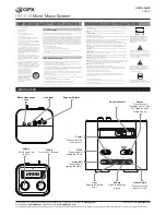
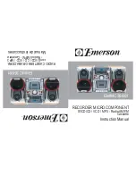
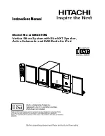
MINI COMPONENT SYSTEM

MODEL

CD-MPX870W Mini Component System consisting of

CD-MPX870W (main unit) and CP-MPX870 (speaker

system).

CONTENTS

Summary of Contents for CD-MPX870W

Page 1: ...upply cord AC plug adaptor 1 2 5 Specifications 1 3 6 Names of parts 1 4 CHAPTER 2 ADJUSTMENTS 1 Mechanism section 2 1 2 Test mode 2 2 3 CD section 2 4 4 CD Changer mechanism section 2 5 CHAPTER 3 MECHANISM BLOCKS 1 Caution on disassembly 3 1 2 Removing and reinstalling the main parts 3 4 CHAPTER 4 DIAGRAMS 1 CD Block diagrams 4 1 2 Main Block diagrams 4 2 CHAPTER 5 CIRCUIT DESCRIPTION 1 Waveforms...

Page 2: ...pairing with conventional lead wire solder may cause damage or accident due to cracks As the melting point of lead free solder Sn Ag Cu is higher than the lead wire solder by 40 C were commend you to use a dedicated soldring bit if you are not familiar with how to obtain lead free wire solder or soldering bit contact our service station or service branch in your area As the melting point of lead f...

Page 3: ...opyrighted works which must not be recorded without the authority of the owner of the copyright Please refer to the relevant laws in your country AC POWER SUPPLY CORD AND AC PLUG ADAPTOR Laser Diode Properties Material GaAIAs Wavelength 795 nm Before operating the unit on mains check the preset voltage If the voltage is different from your local voltage adjust the voltage as follows Turn the selec...

Page 4: ... 150 W 150 W 10 T H D RMS 240 W 120 W 120 W 0 9 T H D Output terminals Speakers 6 ohms Headphones 16 50 ohms recommended 32 ohms Video output 1Vp p Input terminals Game Auxiliary audio signal 500 mV 47 k ohms Game Video 1Vp p Cassette deck Front Speaker Type 5 disc multi play compact disc player Signal readout Non contact 3 beam semiconductor laser pickup D A converter 1 bit D A converter Frequenc...

Page 5: ...icator 3 MP3 WMA Title Indicators 4 MP3 Indicator 5 WMA Indicator 6 Sleep Indicator 7 Timer Play Indicator 8 Timer Recording Indicator 9 Tape 2 Record Indicator 10 MP3 WMA Total Indicator 11 Daily Timer Indicator 12 FM Stereo Mode Indicator 13 FM Stereo Receiving Indicator 14 Tape Play Indicator 15 Memory Indicator 16 Extra Bass Indicator 17 Disc Repeat Play Indicator 18 Disc Pause Indicator 19 Di...

Page 6: ...Stop Button 16 Tape Stop Button 17 Memory Button 18 Disc Pause Button 19 Disc Play or Repeat Button 20 Tape Play Button 21 Tape 2 Record Pause Button 22 Tuning Up Cursor Up Button 23 Disc Track Up or Fast Forward Tape 2 Fast Forward Tuner Preset Up Time Up Cursor Right Button 24 Disc Track Down or Fast Reverse Tape 2 Rewind Tuner Preset Down Time Down Cursor Left Button 25 Tuning Down Cursor Down ...

Page 7: ...lue Play TW 2111 Tape 1 Over 80 g Tape 2 Over 80 g Torque Meter Specified Value Tape 1 Tape 2 Play TW 2111 30 to 80 g cm 30 to 80 g cm Fast forward TW 2231 70 to 180 g cm 70 to 180 g cm Test Tape Adjust ing Point Specified Value Instrument Connection Normal speed MTT 111 Variable Resistor in motor 3 000 30 Hz Speaker Speaker Ter minal Load resistance 6 ohms TAPE MECHANISM Tape Motor Variable Resis...

Page 8: ...Do TOC IL Do normal play When these following key is input into PLAY key track num ber can be appoint directly MEMORY key input 1 key Track 4 2 key Track 9 3 key Track 15 Adjustment result automatically will display as below for each 2 sec a FOF_XXXX b TOF_XXXX c TBAL_XX d TGAN_XX f FGAN_XX g RFLS_XX STOP key input STOP explanation a Focus off set FOF_XXXX b Tracking off set TOF_XXXX c Tracking ba...

Page 9: ...pecific point MEMORY key input Adjustment result automatically will display as below for each 2 sec a FOF_XXXX b TOF_XXXX c TBAL_XX d TGAN_XX f FGAN_XX g RFLS_XX STOP key input STOP explanation a Focus off set FOF_XXXX b Tracking off set TOF_XXXX c Tracking balance TBAL_XX d Tracking Gain TGAN_XX f Focus Gain FGAN_XX g RF level shift RFLS_XX VOL Last memory P GEQ FLAT X BASS OFF To cancel Power OF...

Page 10: ...ile pressing down the button and the button press the GAME VIDEO button The Micro Computer version number will be displayed as CM 3 Press button until WAIT FINISHED appears 4 Unplug the AC cord and the unit is ready for transporting Error Explanation 10 CAM error Can t detect CAM switch when CAM is moving 11 When it detect cam operation error during initialize process 20 TRAY error Can t detect TR...

Page 11: ...CD MPX870W 2 5 4 CD Changer mechanism section All numbers in the drawing correspond to those in parts guide CHANGER MECHANISM PARTS 140 141 HALF GEAR MUST BE ARRANGED AS SHOWN 1 ...

Page 12: ...CD MPX870W 2 6 2 139 APPLY SANKOL SHS1001 BEFORE FIX FIX ITEM 139 ACCORDING TO THE PICTURE AS SHOWN ABOVE ROTATE MODE BIG GEAR UNTIL REACH AS SHOWN IN PICTURE ...

Page 13: ...CD MPX870W 2 7 APPLY GREASE SC141 PULL THE LEVER UNITIL REACH THE ARROW MARK 143 112 3 ...

Page 14: ...CD MPX870W 2 8 FIGURE 1 FIGURE 2 APPLY GREASE SC141 SLOT CLAMP SWITCH ARM INSIDE BASE SLOT HALF GEAR MUST BE ARRANGED AS SHOWN 152 142 118 4 ...

Page 15: ...F GEAR FOLLOW MARKING REFER TO GRAY AREA NO NEED TO APPLY GREASE AT BOTTOM SIDE CORRECT BLACK MARK FIGURE 1 INCORRECT IF DIRECTION IS OTHER THAN DIRECTION SHOWN IN FIGURE 1 IT IS INCORRECT APPLY GREASE SC141 AT TOP SIDE OF GEAR FOLLOW MARKING REFER TO GRAY AREA ...

Page 16: ...CD MPX870W 2 10 APPLY GREASE SC141 AT HALF GEAR AREA ROTATE CLOCKWISE UNTIL REACH HERE MAXIMUM 6 129 ...

Page 17: ...CD MPX870W 2 11 151 150 149 7 ...

Page 18: ...CD MPX870W 2 12 124 131 GREASE SC141 APPLICATION LENGTH GREASE APPLICATION PORTION THE SHOWN AREA MUST FREE FROM GREASE CORRECT INCORRECT SHOWN HOLE MUST FACING ARROW DIRECTION 8 ...

Page 19: ...CD MPX870W 2 13 TR RE JOINT GEAR C APPLY GREASE SC141 AT BOTTOM SIDE ONLY APPLY GREASE SC141 ONLY AT TOP SIDE GEAR MUST BE FIXED ACCORDINGLY TO THE HOLE S 138 126 125 9 ...

Page 20: ...CD MPX870W 2 14 10 148 147 146 145 ...

Page 21: ...CD MPX870W 2 15 APPLY GREASE SC141 WHEN FIXING ITEM 144 MUST FOLLOW AS SHOWN 121 144 130 11 ...

Page 22: ...CD MPX870W 2 16 FIGURE 1 FIGURE 3 FIGURE 2 APPLY GREASE SC141 APPLY GREASE SC141 117 12 ...

Page 23: ...D MPX870W 2 17 ITEM 133 134 MUST APPLY GREASE SC141 ON TOP SIDE GEAR ONLY CORRECT INCORRECT TOP VIEW AFTER BEING ASSEMBLED IT IS INCORRECT TO FIX IT IN REVERSED DIRECTION GEAR 112 GEAR 112 134 133 132 13 ...

Page 24: ...FORE FIX MOVE 112 UNTIL TOUCH THE WALL DURING GEAR A ROTATE MUST PRESS SHOWN AREA AND LEVER B WILL MOVE ARROW DIRECTION THEN FIX PART 108 SCREW TORQUE A B APPLY GREASE SC141 CONFIRM WHETHER FIXED PROPELY OR NOT 108 803 x6 14 2 kgf cm 0 5 0 ...

Page 25: ...CD MPX870W 2 19 APPLY GREASE SC141 BEHIND THE LEVER NEED TO APPLY GREASE SC141 PULL IT THEN LEVER WILL MOVE IN 113 15 ...

Page 26: ...CD MPX870W 2 20 APPLY GREASE SC141 AT BOSS APPLY GREASE SC141 APPLY GREASE SC141 BEFORE FIX SPRING MUST BE ARRANGED UNDER THE HOOK CORRECT LR JOINT LEV LR JOINT LEV BOARD R BOARD R INCORRECT 123 115 16 ...

Page 27: ...LY GREASE SC141 IT IS INCORRECT IF ASSEMBLED IN A REVERSED DIRECTION BIG SLOT MUST FACING OUT WHEN FIX AND AFTER FIXED TO BASE CHASSIS AFTER ASSEMBLY CONFIRM WITH FREE DROP TEST GEAR POSITION DURING FIXING 103 137 136 17 ...

Page 28: ...BLED IN A REVERSED DIRECTION WHEN FIX AND AFTER FIXED TO BASE CHASSIS AFTER ASSEMBLY CONFIRM WITH FREE DROP TEST APPLY GREASE SC141 BIG SLOT MUST FACING OUT GEAR POSITION DURING FIXING CONFIRM BOTH GEARS SIT PROPERLY AND LOCKED 18 104 135 136 ...

Page 29: ...FIRM WHETHER LEVER GO INSIDE THE HOLE OR NOT IT IS INCORRECT IF THE LEVER HOLD DOES NOT ENTER THE HOLE IT IS CORRECT IF THE LEVER HOLD ENTERS THE HOLE 19 ALL OF THIS 135 AND 137 GEAR FIX TOGETHER WITH 119 AND 120 LEVER MOVE TOGETHER BIGGER SLOT FACING OUT 119 135 BIGGER SLOT FACING OUT 120 137 ...

Page 30: ...CD MPX870W 2 24 20 110 BIG SLOT FACING OUT ...

Page 31: ... THE LEVER ACCORDING TO ARROW DIRECTION THEN FIX WHEN FIXING MAIN BASE ASSEMBLY FOLLOW ACCORDING TO PICTURE 1 PICTURE 1 PICTURE 2 PICTURE 3 CORRECT INCORRECT INCORRECT MAKE SURE MECHA HOLDER SHAFT FIX PROPERLY TO LEVER 21 ...

Page 32: ...L SHS1001 INSIDE THE SLOT OTHER SHOWN PORTION APPLY SANKOL SHS1001 AT TRAY SLIDING PORTION FIX TRAY NO 1 FIRST THAN FOLLOW OTHER COSMO GUIDE TRAY HAVE MARKING AS SHOWN 101 102 22 APPLY SANKOL SHS1001 AT BACK PORTION APPLY SANKOL SHS1001 APPLY SANKOL SHS1001 ...

Page 33: ... 27 AFTER ASSEMBLY GEAR UP DOWN BOARD APPLY GREASE SC141 AT INNER OUTER GEAR SLIDING PORTION WHEN FIX GEAR UP DOWN BOARD THE TWO LEVER MUST AT PARALLEL LINE AND POSITIONED AT TOP MAX SIDE 111 23 GEAR UP DOWN BOARD ...

Page 34: ...CD MPX870W 2 28 804 24 SCREW TORQUE ROTATE THE GEAR TO MOVE UP 111 GEAR UP AND DOWN BOARD BEFORE SCREW 3 kgf cm 0 5 0 ...

Page 35: ...OP PLATE FIX THE FFC AFTER FIX PUSH FOLLOW ARROW DIRECTION AFTER PUSH MAKE SURE SNAP PROPERLY BACK PORTION PRESS IN SLOT IN BEFORE LOCK BEFORE LOCK BEFORE LOCK AFTER LOCK AFTER LOCK AFTER LOCK MUST CONFIRM MUST CONFIRM FFC4 122 107 25 ...

Page 36: ...CD MPX870W 2 30 803 26 CORRECT INCORRECT CAUTION 1 MAKE SURE NO PWB CHIP INSIDE SET BEFORE FIX MAKE SURE PWB IS FREE FROM DUST GREASE ETC ...

Page 37: ...IN BASE GREASE SC141 APPLICATION AREA ALL BOSS APPLY GREASE SC141 APPLY GREASE SC141 1 RIB ONLY APPLY GREASE SC141 APPLY GREASE SC141 APPLY GREASE SC141 AT 3 HALF MOON CAUTION TRAY SLIDING AREA MUST FREE FROM GREASE SC141 APPLY GREASE SC141 APPLY GREASE SC141 APPLY GREASE SC141 AT BOTH SLOT APPLY GREASE SC141 INSIDE SLOT APPLY GREASE SC141 AT WALL 105 27 ...

Page 38: ...SCREWING HOLE 13 8 0 2 0 12 2 APPLY GREASE SC141 MUST HAVE GAP REFERENCE ONLY MOTOR GEAR HEIGHT FROM MAIN BASE 12 2 1 5 0 5 0 SCREW TORQUE AFTER SCREW MOTOR CONFIRM THE ARRANGEMENT AS IN FIGURE 2 FIGURE 2 M1 2 801 28 0 1 0 1 ...

Page 39: ...PLY SANKOL SHS1001 3 1 0 1 SHAFT X 3 DIM AFTER INSERTION MUST CONFIRM EVERYDAY SANKOL SHS1001 APPLICATION AREA APPLY GREASE SC141 APPLY GREASE AT THE SLIDING PORTION UP DOWN HOLDER CHANGE TO NATURE COLOR 109 2 29 114 116 ...

Page 40: ...IT MUST FLAT WHEN FITTING STABILIZER PLATE TO STABILIZER ROTATE STABILIZER ANTI CLOCKWISE BY JIG STRICTLY CANNOT FIT USING HAND BY HAND CANNOT X AFTER ASSEMBLED TO HOLDER STABILIZER NEED TO BE CLEANED WITH ALCOHOL DISC TOUCHING SURFACE BELOW 30 ...

Page 41: ...CD MPX870W 2 35 GAP INCORRECT CORRECT INCORRECT APPLY GREASE SC141 MUST MAKE SURE SNAP PROPERLY BOTH SIDE ALL SURFACE MUST TOUCH 106 31 ...

Page 42: ...CD MPX870W 2 36 NO GAP HAVE GAP CORRECT INCORRECT 32 ...

Page 43: ...el Left Right 2 Screw B1 x8 1 3 CD Changer unit 1 Hook C1 x2 2 Socket C2 x1 3 Flat Cable C3 x1 2 4 Rear Panel with Fan motor 1 Screw D1 x9 2 5 Front Panel 1 Screw E1 x3 2 Flat Cable E2 x1 3 Socket E3 x1 4 Hook E4 x2 2 3 2 2 3 6 Main PWB 1 Screw F1 x3 2 Socket F2 x4 2 Socket L3 x1 2 Flat Cable H2 x1 2 Flat Cable L2 x2 2 3 3 7 Power PWB 1 Screw G1 x4 3 8 Tape Mechanism 1 Screw H1 x6 4 9 Game Input P...

Page 44: ... x1 Changer Mechanism Unit N1 x4 2 6x10mm Changer Mechanism Unit CD Mechanism Figure 6 Figure 8 Figure 7 Figure 4 H1 x6 Mechanism Tape H2 x1 Lug wire Front Panel Figure 5 Game Input PWB J1 x2 K1 x1 K4 x6 2 6x10mm Special Display PWB Washer K3 x1 Nut K2 x1 Front Panel 3x10mm O 3x10mm O O O O ...

Page 45: ...Panel A1 x1 9 2 Tweeter 1 Screw B1 x2 1 Screw C1 x2 4 Screw A4 x4 3 Screw A3 x2 2 Socket A2 x1 3 Super tweeter 3x10mm 3x10mm 4x16mm WOOFER A4 x4 Front Panel Figure 9 C1 x2 B1 x2 Speaker Box A1 x1 SUPER TWEETER TWEETER Screwdriver 3x10mm LED PWB A3 x2 A2 x1 O O O O ...

Page 46: ...en installing the pinch roller pay attention to the spring mounting position Figure 3 1 4 How to remove the belt TAPE 2 See Fig 4 1 Remove the main belt D1 x 1 pc from the motor side 2 Remove the FF REW belt D2 x 1 pc 1 5 How to remove the belt TAPE 1 See Fig 4 1 Remove the main belt E1 x 1 pc from the motor side 2 Remove the FF REW belt E2 x 1 pc Figure 4 1 6 How to remove the motor See Fig 5 1 R...

Page 47: ...ition then rotate further to eject the disc tray so that CD can be removed from the tray Figure 2 Figure 3 2 In another case if CD mechanism is at tray No 1 play position and to remove CD located in tray No 3 the procedure is as follows If the gear up down board is located at tray No 1 position then rotate gear clock wise until it at stock position Rotate reduction gear D clockwise Figure 4 to mov...

Page 48: ...n cam motor 5 Changer Motor PWB Figure 1 NOTE There are 2 more screws tighten the motors at the bottom of main chassis Before performing procedure 1 above disc stop spring top plate sear up down board and trays must be removed then only the 2 screws can be untighten 5 Changer Motor PWB Tray Motor Changer Mechanism Unit Main Cam Motor A1 X2 φ2x10mm ...

Page 49: ... 41 AVDD XIN XOUT INTB1 INTB0 RESB DO DI CL CE TO DISPLAY SECTION TO MAIN SECTION CNP3 CNP7 M1 TRAY MOTOR MGND PICKUP UNIT IN PICKUP NSW 1 MOTOR SPINDLE NM1 MOTOR SLED NM2 COIL TRACKING FOCUS COIL 16 9344 MHz XL1 5V DRIVER LASER 3 3V CONSTANT VOLTAGE 3 3V 3 3V Q1 R CH AGND L CH D_ 5V B5 B6 GND PHOTO MO_A CD_RESB MO_A CD_DI CD_DO CD_CLK CD_CE 8V B7 7 27 9 28 17 15 13 11 23 22 32 33 31 34 30 19 20 2...

Page 50: ...09 BIAS OSC Q111 L103 Q105 Q106 REC P B HEAD TAPE 2 P B HEAD TAPE 1 R CH L CH R CH L CH IC601 LC75341 AUDIO PROCESSOR B4 R L REC R L ALC R REC L REC POPREDUCE SWITCHING L T2 R T2 R T1 L T1 21 4 24 2 1 18 11 16 3 15 10 9 7 23 14 12 13 19 7 18 10 43 5 13 21 4 2 24 23 6 9 16 12 11 15 1 H N P B REC T1 T2 T1 T2 NOR HIGH B4 B4 B4 SYSTEM MUTE TAPE MECHANISM ASS Y MOTOR DRIVER SOLENOID DRIVER B3 B3 LED701...

Page 51: ...N IC701 IXA101AW SYSTEM MICROCOMPUTER 1 2 FL701 FL DISPLAY 26 51 50 81 8 1 545152531011 14 18 2 78 57 8 1 2 4 5 3 2 1 11 6 7 1 5 8 98 100 99 2 4 34 32 25 18 B8 VDD 79 16 17 42 13 12 20 23 28 29 30 31 36 80 26 38 37 39 40 55 15 14 27 41 T F PT801 MAIN POWER TRANSFORMER SYSTEM MUTE TAPE MECHANISM ASS Y RESET SP DET SP RELAY ON OFF FAN MOTOR DRIVER TER RELAY DRIVER D856 1SS119 IC854 KIA78L05 3 2 1 VO...

Page 52: ...EDGE CH2 Delay 2 924 ms Hold off 0 2 µs CH3 0 00 V CH4 0 00 V BW FULL Trigger Filter Offset 1 IC1 22 5 IC1 25 Vp p 1 0 V 1 3 V 0 5 mV div 0 5 µsec div 4 IC1 2 T FDO TE Stopped CH1 500 mV DC 10 1 CH2 10 V DC 10 1 CH3 1 V DC 10 1 500 ms div 500 ms div NORM 20 kS s 1 2 3 Record Length Smoothing ON CH1 0 000 V CH2 0 0 V Main 100 K Zoom 2 K Mode AUTO Type EDGE CH1 Delay 0 0 ns Hold off 0 2 µs CH3 0 00 ...

Page 53: ...4 0 18 0 46 0 12 0 5 2 49 47 1 45 13 6 9 6 2 69 48 1 49 14 4 18 7 1 34 PIN 49 3 19 15 0 8 12 66 NO 50 3 79 16 3 45 1 5 06 17 0 6 2 12 83 18 0 3 19 6 19 2 59 4 0 20 2 5 18 28 21 2 6 9 92 22 0 7 8 4 23 0 24 0 IC 851 VOLTAGE IC 503 IC 901 VOLTAGE IC101 IC2 VOLTAGE VOLTAGE IC1 IC 601 VOLTAGE VOLTAGE PIN PIN VOLTAGE NO NO 1 4 94 V 4 94 V 4 92 V 4 92 V 1 32 V 4 92 V 4 92 V 51 2 52 4 40 V 4 38 V 4 39 V 4...

Page 54: ...CD MPX870W 5 3 MEMO ...

Page 55: ...on is the one measured by Digital Multimeter between such a section and the chassis with no signal given 1 In the tuner section indicates AM indicates FM stereo 2 In the main section a tape is being played back 3 In the deck section a tape is being played back indicates the record state 4 In the power section a tape is being played back 5 In the CD section the CD is stopped Parts marked with are i...

Page 56: ...CD MPX870W 6 2 3 Schematic diagram Figure 6 2 MAIN SCHEMATIC DIAGRAM 1 2 ...

Page 57: ...CD MPX870W 6 3 Figure 6 3 MAIN SCHEMATIC DIAGRAM 2 8 ...

Page 58: ...CD MPX870W 6 4 Figure 6 4 POWER SCHEMATIC DIAGRAM 3 8 ...

Page 59: ...CD MPX870W 6 5 Figure 6 5 POWER SCHEMATIC DIAGRAM 4 8 ...

Page 60: ...CD MPX870W 6 6 Figure 6 6 DISPLAY SCHEMATIC DIAGRAM 5 8 ...

Page 61: ...CD MPX870W 6 7 Figure 6 7 DISPLAY SCHEMATIC DIAGRAM 6 8 ...

Page 62: ...CD MPX870W 6 8 Figure 6 8 CD SERVO SCHEMATIC DIAGRAM 7 8 ...

Page 63: ...CD MPX870W 6 9 Figure 6 9 CD SERVO SCHEMATIC DIAGRAM 8 8 ...

Page 64: ...CD MPX870W 6 10 4 Wiring side of PWB Figure 6 10 WIRING SIDE OF MAIN PWB TOP VIEW 1 15 ...

Page 65: ...CD MPX870W 6 11 Figure 6 11 WIRING SIDE OF MAIN PWB TOP VIEW 2 15 ...

Page 66: ...CD MPX870W 6 12 Figure 6 12 WIRING SIDE OF MAIN PWB BOTTOM VIEW 3 15 ...

Page 67: ...CD MPX870W 6 13 Figure 6 13 WIRING SIDE OF MAIN PWB BOTTOM VIEW 4 15 ...

Page 68: ...CD MPX870W 6 14 MEMO ...

Page 69: ...CD MPX870W 6 15 Figure 6 14 WIRING SIDE OF POWER PWB 5 15 ...

Page 70: ...CD MPX870W 6 16 Figure 6 15 WIRING SIDE OF DISPLAY PWB TOP VIEW 6 15 ...

Page 71: ...CD MPX870W 6 17 Figure 6 16 WIRING SIDE OF DISPLAY PWB TOP VIEW 7 15 ...

Page 72: ...CD MPX870W 6 18 Figure 6 17 WIRING SIDE OF DISPLAY PWB BOTTOM VIEW 8 15 ...

Page 73: ...CD MPX870W 6 19 Figure 6 18 WIRING SIDE OF DISPLAY PWB BOTTOM VIEW 9 15 ...

Page 74: ...CD MPX870W 6 20 Figure 6 19 WIRING SIDE OF GAME INPUT PWB TOP VIEW 10 15 ...

Page 75: ...CD MPX870W 6 21 Figure 6 20 WIRING SIDE OF GAME INPUT PWB BOTTOM VIEW 11 15 ...

Page 76: ...CD MPX870W 6 22 Figure 6 21 WIRING SIDE OF CD SERVO PWB TOP VIEW 12 15 ...

Page 77: ...CD MPX870W 6 23 Figure 6 22 WIRING SIDE OF CD SERVO PWB TOP VIEW 13 15 ...

Page 78: ...CD MPX870W 6 24 Figure 6 23 WIRING SIDE OF CD SERVO PWB BOTTOM VIEW 14 15 ...

Page 79: ...CD MPX870W 6 25 Figure 6 24 WIRING SIDE OF PWB 15 15 ...

Page 80: ... Spin system check 4 PLL system check 5 Others Parts code 1 CD optical pickup Lens cleaner disc UDSKA0004AFZZ HOW TO USE CAUTION Cleaning fluid Cleaner disc Using the brush in the cleaner cap apply 1 or 2 drops of the cleaning fluid to the brush on the CD cleaner disc which has the mark next to it Place the CD cleaner disc onto the CD disc tray with the brush side down then press the play button Y...

Page 81: ...1 No Check the focus peripheral circuit Yes 3 Is the laser lit No Check the laser diode driver Q1 peripheral circuit Yes 4 Is the turntable rotating No Spindle motor NM1 When a disc is loaded start playback operation 1 Is focus servo activated Waveform drawing Figure 2 No Pins 5 9 11 18 and 19 on IC1 Check the laser diode driver Q1 peripheral circuit Yes 2 Is the HF waveform normal Waveform drawin...

Page 82: ...100 ms div NORM 100 kS s 2 1 Record Length Smoothing ON CH1 0 0 V CH2 0 00 V Main 100 K Zoom 2 K Mode NORMAL Type EDGE CH1 Delay 2 924 ms Hold off 0 2 µs CH3 0 00 V CH4 0 00 V BW FULL Trigger Filter Offset 3 Spin system check Press the OPEN CLOSE switch without inserting a disc and then try starting the play operation 1 The turntable rotates a little Waveform drawing Figure 5 Yes The spin driver c...

Page 83: ...ode AUTO Type EDGE CH2 Delay 0 0 ns Hold off 0 2 µs CH3 0 00 V CH4 0 00 V BW FULL Trigger Filter Offset CH1 v DIV 500 mV 1999 04 05 17 33 17 5 Others Is pin 35 C2F on IC1 L No There are too many error flags on a damaged disc which makes error correction impossible Yes 1 When playing at normal speed Check the peripheral circuit at pin 69 DOUT on IC1 and the waveform Figure 7 Check again using a kno...

Page 84: ...er output 26 VVSS1 For use by the EFM PLL Circuit Built in VCO GND pin This pin must always be connected to 0V 27 PDOUT1 Output UNSTABLE Phase comparison output pin 1 to control built in VCO 28 PDOUT0 Output UNSTABLE Phase comparison output pin 0 to control built in VCO 29 PCKIST Input INPUT Resistor connection pin to set current for PDOUT 0 and 1 output 30 VVDD1 Built_in VCO power supply pin 1 31...

Page 85: ...el data output pin 61 VVDD2 For use by the EFM PLL Circuit Built in VCO power supply pin 2 62 VPREF2 Input INPUT Built in VCO control oscillator range setting input pin 63 VCOC2 Input INPUT Built in VCO control voltage setting input pin 64 VPDOUT2 Output UNSTABLE Built in VCO control output pin 2 65 VVSS2 Built in VCO GND pin This pin must always be connected to 0V 66 DVDD1 8 Output H Supply volta...

Page 86: ...VSS RCH0 AVDD SLC0 LC78690E VVDD2 VPREF2 VCOC2 VPDOUT2 VVSS2 DVDD1 8 DVSS DVDD DOUT AMUTEB XVSS XOUT XIN XVDD LCH0 LRVDD LRVSS RCH0 AVDD SLC0 EFMIN RFOUT LPF PHLPF AIN CIN BIN DIN FEC RFMON VREF JITTC EIN FIN TEC TE TEIN AVSS LDD LDS AVDD FD0 TD0 SLD0 SPD0 VVSS1 PDOUT1 PDOUT0 PCKIST VVDD1 DMUTEB PUIN DEFECT FSEQ C2F DVDD DVSS VVDD3 VVSS3 DVDD1 8 DVDD DVSS CE CL DI DO RESB INTB0 INTB1 CONT2 CONT1 C...

Page 87: ... Input pin for channel 2 14 VIN2G Input pin for channel 2 for gain control 15 VIN3 Input pin for channel 3 16 VIN3G Input pin for channel 3 for gain control 17 VIN4 Input pin for channel 4 18 VIN4G Input pin for channel 4 for gain control 19 FWD5 CH5 Output change pin FWD Logic input for bridge 20 REV5 CH5 Output change pin REV Logic input for bridge 21 VCONT5 Input pin for CH5 output voltage cont...

Page 88: ...5 16 17 18 36 35 34 33 32 31 30 29 28 27 26 25 24 23 22 21 20 19 11k 22k 1k 1k 1k 1k 11k 11k 11k 22k 22k 22k Pre Drive Pre Drive Reference voltage DUFFER AMP For 1 2 VCC DUFFER AMP For VREF TSD Band gad BTL Mode select Mode select CH4 CH5 CH6 CH3 CH2 CH1 VOLTAGE CONTROL AMP Figure 8 5 BLOCK DIAGRAM OF IC ...

Page 89: ... 16 R1 4 Input signal pin 17 RSEL0 Input selector output pin 18 RIN Volume equalizer output pin 19 RTRE Treble band filter comprising capaci tor and resistor connection pin 20 RBASS Bass band filter comprising capaci tor and resistor connection pin 21 ROUT Bass band filter comprising capaci tor and resistor connection pin and bass treble output pin 22 VREF 0 5x VDD voltage generation block for ana...

Page 90: ...ted to the IC substrate 5 MODE 1 REG1 REG2 REG3 and REG4 outputs are turned ON when this pin is 5 V 6 REG2 Output 10 V power supply with a minimum peak out current of 800 mA 7 REG1 Output 8 5 V power supply with a minimum peak out current of 700 mA 5 2 3 4 1 7 6 Peak Current Protection Thermal Protection Load Short Protection Out puts Prc Drive Prc Drive Prc Drive Prc Drive Referenc e Voltage MODE...

Page 91: ... 1g 1p 1e 1n 1r 1c 2a 2b 1b 2j 2k 2h 2f 2m 2d 2g 2p 2e 2n 2r 2c 1a 1j 1k 1h 1f 1m 1d 1g 1p 1e 1n 1r 1c 2a 2b 1b 2j 2k 2h 2f 2m 2d 2g 2p 2e 2n 2r 2c 1a 1j 1k 1h 1f 1m 1d 1g 1p 1e 1n 1r 1c 2a 2b 1b 2j 2k 2h 2f 2m 2d 2g 2p 2e 2n 2r 2c 1a 1j 1k 1h 1f 1m 1d 1g 1p 1e 1n 1r 1c 2a 2b 1b 2j 2k 2h 2f 2m 2d 2g 2p 2e 2n 2r 2c 1a 1j 1k 1h 1f 1m 1d 1g 1p 1e 1n 1r 1c 2a 2b 1b 2j 2k 2h 2f 2m 2d 2g 2p 2e 2n 2r 2c ...

Page 92: ...CD MPX870W 8 9 MEMO ...

Page 93: ...ining the safety and performance of the set This document has been published to be used for after sales service only The contents are subject to change without notice 1 INTEGRATED CIRCUITS 2 TRANSISTORS 3 DIODES 4 VIBRATORS CRYSTALS 5 TRANSFORMERS 6 COILS 7 CAPACITORS 8 RESISTORS 9 OTHER CIRCUITRY PARTS 10 CD MECHANISM PARTS 11 CHANGER MECHANISM PARTS 12 CABINET PARTS 13 SPEAKER BOX PARTS 14 ACCES...

Page 94: ... Digital PNP KRA107 S Q706 VSKRC104S 1 AC Digital NPN KRC104 S Q707 VSKRA107S 1 AB Digital PNP KRA107 S Q708 VSKRC104S 1 AC Digital NPN KRC104 S Q709 VSKTA1273Y 1 AE Silicon PNP KTA1273 Y Q710 VSKTA1273Y 1 AE Silicon PNP KTA1273 Y Q711 VSKTA1273Y 1 AE Silicon PNP KTA1273 Y Q712 VSKRC102S 1 AB Digital NPN KRC102 S Q713 VSKRC104S 1 AC Digital NPN KRC104 S Q801 VSKTA1274Y 1 AE Silicon PNP KTA1274 Y Q...

Page 95: ...µ H 7 CAPACITORS C1 VCEAZA1AW107M AB 100 µ F 10V Electrolytic C2 VCKYCY1HB102K AA 0 001 µ F 50V C3 VCEAZA1AW107M AB 100 µ F 10V Electrolytic C4 VCKYPA1HB103K AA 0 01 µ F 50V C5 VCEAZA1EW476M AB 47 µ F 25V Electrolytic C6 RC EZ0004AWZZ AD 3 3 µ F 16V Electrolytic C7 VCKYPA1HB102K AA 0 001 µ F 50V C8 VCEAZA1AW476M AB 47 µ F 10V Electrolytic C9 VCKYCY1HB103K AA 0 01 µ F 50V C10 VCEAZA0JW108M AC 1000 ...

Page 96: ... 22 µ F 25V Electrolytic C134 VCEAZA1AW227M AC 220 µ F 10V Electrolytic C135 VCKYCY1EF223Z AB 0 022 µ F 25V C137 VCQYKA1HM473K AB 0 047 µ F 50V Mylar C138 VCQPKA2AA822J AA 0 0082 µ F 100V C139 VCQYKA1HM393K AB 0 039 µ F 50V Thin Film C140 VCEAZA1EW476M AB 47 µ F 25V Electrolytic C141 VCEAZA1CW107M AC 100 µ F 16V Electrolytic C143 VCEAZA1HW335M AB 3 3 µ F 50V Electrolytic C150 VCEAZA1EW476M AB 47 µ...

Page 97: ...µ F 50V C904 VCKYCY1HB102K AA 0 001 µ F 50V C905 VCEAZA1HW476M AB 47 µ F 50V Electrolytic C906 VCEAZA1HW476M AB 47 µ F 50V Electrolytic C907 VCCCCY1HH101J AA 100 p F CH 50V C908 VCCCCY1HH3R0C AA 3 p F CH 50V C909 VCQYKA1HM104K AB 0 1 µ F 50V Mylar C910 VCCCCY1HH3R0C AA 3 p F CH 50V C911 VCEAZA2AW107M AD 100 µ F 100V Electrolytic C912 VCEAZA2AW107M AD 100 µ F 100V Electrolytic C913 VCCCCY1HH101J AA...

Page 98: ...8x1 55mm Green JP823 VRS CY1JB000J AA 0 ohms Jumper 0 8x1 55mm Green R7 VRD ST2CD470J AA 47 ohms 1 6W R8 VRS CY1JB100J AA 10 ohms 1 16W R9 VRD ST2CD102J AA 1 kohms 1 6W R10 VRD ST2CD562J AA 5 6 kohms 1 6W R11 VRD ST2CD682J AA 6 8 kohms 1 6W R12 VRD ST2CD103J AA 10 kohms 1 6W R13 VRD ST2CD103J AA 10 kohms 1 6W R14 VRS CY1JB103J AA 10 kohms 1 16W R15 VRS CY1JB103J AA 10 kohms 1 16W R16 VRS CY1JB331J...

Page 99: ... CY1JB184J AA 180 kohms 1 16W R137 VRS CY1JB184J AA 180 kohms 1 16W R138 VRS CY1JB103J AA 10 kohms 1 16W R139 VRS CY1JB103J AA 10 kohms 1 16W R140 VRS CY1JB473J AA 47 kohms 1 16W R141 VRS CY1JB472J AA 4 7 kohms 1 16W R142 VRD RT2HD820J AA 82 ohms 1 2W R143 VRS CY1JB473J AA 47 kohms 1 16W R144 VRS CY1JB223J AA 22 kohms 1 16W R145 VRD ST2CD4R7J AA 4 7 ohms 1 6W R146 VRS CY1JB103J AA 10 kohms 1 16W R...

Page 100: ...S CY1JB103J AA 10 kohms 1 16W R754 VRD ST2EE331J AA 330 ohms 1 4W R756 VRD ST2CD182J AA 1 8 kohms 1 6W R757 VRS CY1JB102J AA 1 kohms 1 16W R758 VRS CY1JB102J AA 1 kohms 1 16W R759 VRD ST2CD122J AA 1 2 kohms 1 6W R760 VRS CY1JB103J AA 10 kohms 1 16W R761 VRS CY1JB103J AA 10 kohms 1 16W R762 VRS CY1JB103J AA 10 kohms 1 16W R763 VRD ST2CD103J AA 10 kohms 1 6W R764 VRS CY1JB472J AA 4 7 kohms 1 16W R76...

Page 101: ...R949 VRD RT2HD102J AA 1 kohms 1 2W R950 VRD ST2CD683J AA 68 kohms 1 6W R956 VRS CY1JB102J AA 1 kohms 1 16W R958 VRG ST2EC101J AB 100 ohms 1 4W Fusible R968 VRD ST2CD223J AA 22 kohms 1 6W R983 VRS CY1JB333J AA 33 kohms 1 16W R984 VRS CY1JB821J AA 820 ohms 1 16W R985 VRS CY1JB822J AA 8 2 kohms 1 16W R986 VRS CY1JB822J AA 8 2 kohms 1 16W R987 VRS CY1JB222J AA 2 2 kohms 1 16W R988 VRS CY1JB222J AA 2 2...

Page 102: ...at Cable 7Pin FFC703 QCNWN2717AWPZ AD Flat Cable 11Pin FL701 VVKNA12MM54 1 AU FL Display FW901 QCNWN2711AWPZ AD Flat Wire JK690 QSOCJ0313AWZZ AF Jack Game Input JK691 QSOCJ0120AWZZ AD Jack Video Out JK692 QJAKM0004AWZZ AK Jack Headphones JOG701 QSW ZA001AWZZ AE Volume Variable LG1 QLUGPA001AWZZ AC Lug Terminal LG2 QLUGPA001AWZZ AC Lug Terminal LG3 QLUGPA001AWZZ AC Lug Terminal LG4 QLUGPA001AWZZ AC...

Page 103: ...CD MPX870W 10 MEMO ...

Page 104: ...CD MPX870W 11 10 CD MECHANISM PARTS ...

Page 105: ...shion 306 92LHPC1LVASY AZ Pickup Unit Ass y 306 1 Pickup Unit Not Replacement Item 306 2 NGERR0043AFZZ AC Gear Rack 306 3 MSPRC0961AFZZ AA Spring Rack 307 PCUSG0001AWSA AD Cushion 308 PCUSG0004AWSA AD Cushion 701 XBSY726P06000 AA Screw M2 6x6mm 703 XBBY720P03000 AA Screw M2x3mm 704 LX WZ1070AFZZ AA Washer M1 5xM3 8x0 25mm M1A 92LMTR6447CASY AQ Motor with Chassis Spindle M2A 92LMTR6447BASY AN Motor...

Page 106: ...CD MPX870W 13 11 CHANGER MECHANISM PARTS ...

Page 107: ...NGERH0179AWZZ AC Tray Rear Gear A 128 NGERH0180AWZZ AB Tray Rear Gear B 129 NGERH0181AWZZ AC Mechanism Clamp Gear A 130 NGERH0182AWZZ AC Mechanism Clamp Joint Gear 131 NGERH0183AWZZ AC Mechanism Clamp Board Gear 132 NGERH0184AWZZ AC Tray Rear Joint Gear A 133 NGERH0185AWZZ AC Tray Rear Joint Gear B 134 NGERH0186AWZZ AC Tray Rear Joint Gear C 135 NGERH0187AWZZ AB Tray Rear Drive Gear 136 NGERH0188A...

Page 108: ...CD MPX870W 15 12 CABINET PARTS ...

Page 109: ...nger Unit 208 92LNBAND1318A AA Nylon Band 80mm 209 KMECBA012AWZZ BB Tape Mechanism Ass y 210 HDECQ1110AWSA AF Panel Edge Light 211 QCNWN1860AWZZ AC Lug Wire 212 JKNBKA022AWSB AL Knob Volume 213 92LCSPR1431C AA Spring Ring 214 LCHSMA044AWFW AR Chassis Main 215 LBND 1011AWZZ AA Nylon Band 216 QACCA001AW00 AP AC Power Supply Cord For Latin of America 216 QACCL0008AW00 AN AC Power Supply Cord For Aust...

Page 110: ...CD MPX870W 17 13 SPEAKERS BOX PARTS ...

Page 111: ...olyethylene Bag Accessories 8 SPAKP0032AWZZ AF Polyethylene Bag Unit 9 SSAKHA077AWZZ AD Polyethylene Bag Speaker 10 TINSZA205AWZZ AM Operation Manual 11 TLABZA267AWZZ AB Label WMA 12 TLABZA392AWZZ AD Label Pop Tape 1 13 TLABZA368AWZZ AD Label Pop Tape 2 14 TLABZA329AWZZ AB Caution Battery For Australia New Zealand only 15 SPAKP0026AWZZ AB Polyethylene Bag AC Cord For Argentine only 16 TLABSA040AWZ...

Page 112: ...CD MPX870W 19 ...

Page 113: ...CD MPX870W 22 MEMO ...

Page 114: ...CD MPX870W 20 ...

Reviews: