background image


INDEX TO CONTENTS


Summary of Contents for CD-JX20X(GY)

Page 1: ...NS ON HANDLING THE UNIT NAMES OF PARTS OPERATION MANUAL DISASSEMBL REMOVING AND REINSTALLING THE MAIN PARTS ADJUSTMENT TROUBLESHOOTING CD SECTION FUNCTION TABLE OF IC BLOCK DIAGRAM LCD SEGMENT TYPES OF TRANSISTOR AND LED NOTES ON SCHEMATIC DIAGRAM WAVE FORMS OF CD CIRCUIT SCHEMATIC DIAGRAM WIRING SIDE OF P W BOARD EXPLODED VIEW REPLACEMENT PARTS LIST Page 2 2 2 3 5 6 12 13 15 16 17 18 22 23 26 27 ...

Page 2: ...tional speed 200 500 rpm CLV Approx Error correction CIRC Cross Interleave Reed So lomon Code Audio channels 2 Decoder i6 bit linear quantization Filter 4 times oversampling 16 bit digi tal filter Frequency response 20 20 000 Hz i 3 dB Wow and flutter Unmeasurable less than 0 001 W peak Specifications for this model are subject to change without prior notice QACCL0059AFOO For Australia QACCK0053AF...

Page 3: ...n Power Indicator 33 Timer Sleep Indicator 34 FM Stereo Indicator n Tape control section 35 Reverse Play Button and Indicator 4 36 Stop Button B 37 Forward Play Button and Indicator b 38 Record Pause Button and Indicator 0 I I 39 Fast Wind APSS Buttons M w 40 One Touch Editing Buttons 41 Tape Mode Button and Indicators 1 Reverse Mode Switch 2 Timer Record Switch 3 FM Mode Switch 4 Funcbon Selector...

Page 4: ...a soft cloth l Exposmg the sensor on the ma un t to strong light can interfere with operation Change lighting or the dfrectlon of the I l Keep the remote conlrol away from moisture excessive heat shock and vrbralions l The remote controlls usable range IS between 0 2 m 0 7 feet and 6 m 20 feet away from the sensor l Whilst the frequency Indicator on the tuner or the ON TIME in dicator IS 11t press...

Page 5: ...button and load the CD to be recorded 3 Load a cassette into the TAPE 2 cassette compartment 0 Wind the beginning part of the tape on which recording can not be performed z 4 Set the REVERSE MODE switch to z to record on only one side or to 3 for continuous recording on both sides 5 Press the REC PAUSE 011 button 0 The REC PAUSE indicatdrjights up and the PLAY indicators flash 6 Press the PLAY REP...

Page 6: ...to adjust the time minute by minute 0 ClO to C99 can be set 7 Press the AUTO EDIT button 0 Tracks on the CD are automatically divided between side A and side 0 0 The number of tracks total time and track numbers to be recorded on side A and side B are displayed for approximately 4 seconds When there are tracks which can not be recorded the TIME OVER indicator will light up 8 Press the PLAY REPEAT ...

Page 7: ...DIT button 0 Press NORMAL to edit at normal speed and HIGH to edit at twice the normal speed 0 Editing will begin with side A To stop dubbing Press the STOP U button 0 TAPE 1 and TAPE 2 simultaneously stop After dubbing The indicator of the TAPE 1 2 button is automatically switched to 2 Only when the tape is rewound and played back the contents currently dubbed can be confirmed Synchro reverse edi...

Page 8: ...r C whichever gives the best reception n Erasing recorded tapes APSS requires blanks of 4 5 seconds between selections to function properly Make the blanks as follows 1 Press the REC PAUSE all button when the selection being recorded ends 2 Press the AUX button Note Du not connect anything to the AUX sockets 3 Press the PLAY b or PLAY 4 button of which its indi cator is lit let the tape run for 4 ...

Page 9: ...the preset time t i n W Sleep operation The radio compact disc and cassette deck can all be automatically turned off after 60 minutes Press the SLEEP button To stop the sleep operation Press the SLEEP button The SLEEP indicator wll go out To record radio programmes You can record a broadcasting station different from that to which you are listening However the band should be the same 1 Load a blan...

Page 10: ...1 x5 13 2 14 i 2 Socket 62 x2 14 Z I CD sew0 PWB 1 Screw Ci x4 14 2 2 Socket C2 xl 3 Flexible PWB C3 xl 2 CD mechanism 1 Screw 1 x3 14 2 Frame with PWB 1 Screw El x3 13 2 14 l 2 Socket lEZlx5 14 3 5 Tape mechanism 1 Screw fF11x3 14 5 2 Socket iF2ix4 14 4 5 LCD PWB 1 Screw Gl x6 14 1 2 Socket GZ x2 3 Connector G3 xl 6 CD switch PWB 1 Knob ftillxl 14 s Following the disassembling procedure steps 1 a...

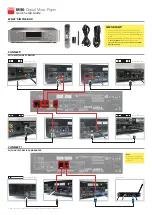
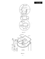
Page 11: ...Figure 15 1 Rear cabinet ILeft Side Figure 15 2 15 ...

Page 12: ..._ Motor Motor See Fig 16 2 3 1 Remove the screw Bl x 4 PCS and remove the motor fixture 2 Remove the screw B2 x 3 PCS and remove the motor Note 1 When mounting the motor pay attention to the motor mounting angle 2 When the motor is removed the belt comes off Put it on referring to the description of belt putting on Switch PWB See Fig 16 4 1 Remove the screw Cl x 2 PCS and remove the switch protect...

Page 13: ...rase Head See Fig 17 2 4 1 Remove the screw Fl x 2 PCS and remove the head base 2 Remove the screw F2 x 2 PCS and remove the head Cares When Mounting the Head Mount the head in the position shown in Fig 17 4 Be sure to apply screw lock after replacement of head and azimuth adjustment CD MECHANISM SECTION Removing the optical pickup See Fig 17 5 1 Remove 4 pawls Gl and remove cover G2 2 Remove 4 sc...

Page 14: ...f each switch or control Volume Beat cancel Bass Tone Function FM modenape selector Max A Center Center Tape Stand by Stereo Normal i l Bias Oscillation Check Specified value Beat cancel A 104 77 kHz B 4 2 kHz for A C Same as A I l Erase Current Check Specified value Resistor for measurement Normal 75 i 30 mV 1 ohm Cr02 100 f 30 mV t Metal 175 i 35 mV l Head Azimuth Test Tape Ml T 114 Instrument C...

Page 15: ...l oscillator Setting Adjusting part No modulation VU2 19 kHz 100 Hz l Adjusting signals Frequency Modulation Modulation Antenna input frequency factor level TI FM monaural 98MHz FM stereo 400Hz 225kHzdev 60dB 98MHz 1 OOOHz 1 160dB 1Max frequency deviation is 67 5 kHzdev in case of SSG output mode MAIN Frequency deviation caused only by SSG pilot signal is 7 5 kHzdev ELECTRONIC AM SIGNAL BAR ANTENN...

Page 16: ...me are indicated Use the disc T t t t Display Da lE51 j L 1 I r l i After TEST MODE 5 the PLAY button is inoperative Even when it is pressed 6th time key entry IS not accepted Unless the CD lid switch SW303 is turned on the test mode is not set Button Operation in Test Mode 1 When the STOP button is pressed all operations stop At this time the optical pickup does not slide and TEST MODE 0 is displ...

Page 17: ...6 Pin 6 1 2Vcc and pin 4 TGI nf TP K 7 Figure 22 1 I I II I 1 Adjust to obtain vertically symmetrical waveform Fig 21 I with respect to reference DC level The reference level is l ZVcc Amplitude of 0 5 to 1 5 Vpp 2 Input oscillation frequency 1 3 kHz 100 mV rms 3 Input oscillation frequency 1 5 kHz 300 mV rms 4 Watch the monitor Adjust so that the error waveform is uniform and minimum Fig 22 2 and...

Page 18: ... Check between pin 17 of CNP851B and Q890 base If OK 0890 is defective 1 Yes ___ Is there 5 V at pin 5 of CNP700 k The PWB pattern between 0890 and pin 5 of CNP700 is damaged 1 Yes 1 Check the CNP700 and Flexible PWB If they are normal the pickup is defective A mcus When the disc is removed is the Check the item of 7he saw tooth wave for focus servo does pickup mowng up and down Is the focus gain ...

Page 19: ...l of TP751 No Check the CNP700 flexible PWB and NICl If OK the pickup is defective Normal I Is the tracking gain adjusting VR750 set to the minimum position Check the connection between pin 9 of CNP700 and pin 3 TEIN of IC750 or pin 4 TGl of TP751 and the F Readjust the tracking gain Yes 1 F Check the peripheral parts of IC750 If OK IC750 is defective No Is there any output between pins 11 and 14 ...

Page 20: ...C750 and pin 15 of IC720 l 2 Vcc No Check the peripheral parts of IC750 If OK IC750 is defective IS the slide feed signal being output between pins 3 and 6 of IC720 Check the connection between pin 8 of IC720 and pin 25 SS OUT of No IC750 If OK IC720 is defective Is the slide feed voltage being supplied to the both ends of the slide motor 1 Yes No Check the CNP720 and flexible PWB and then connect...

Page 21: ...WMDAC clock and clock to read the digital audio data into LSI as bit serial data 10 VDD Input Power voltage terminal 5 V 11 TSTOUT output Test output terminal Ordinarily it is open 12 TSTl Input Test output terminal Ordinarily it is connected to GND 13 TST2 InDut Test outout terminal Ordinarily it is connected to GND 14 IF Input Interface switching terminal MSB first When digital audio data input ...

Page 22: ...indicator H OFF goes out L ON lights L N DUB IND Constant speed dubbing indicator H OFF goes out L ON lights L Tl IND Tl indicator H OFF goes out L ON lights L T2 IND T2 indicator H OFF goes out L ON lights L 25 TEST Input _ Test terminal Open or GND 26 vss GND Earth L 27 VDD Input VDD Power supply 28 P20 output PAUSE IND PAUSE indicator H OFF goes out ON lights L 36 j RBO output Key matrix output...

Page 23: ...tion L is outputted in REC standby mode L 55 56 57 58 59 60 61 62 l 1 63 1 R91 Input SY ON R92 Input Output CK RCO Input RDY RCl Input DATA RC2 RC3 Input TM REC VDD Input VDD RDO Input RV MOD2 RDI Input RV MOD1 Synchronizing signal detection H REC run L REC standby H Remote control request signal READY signal from remote control decoder L Remote control serial data Not used Timer REC switch detect...

Page 24: ...speed reduction signal brake control Switch input to detect position of optical pickup L When the pickup exists on the innermost periphery of disc When the pickup does not exist on the innermost periphery of I TIMER ON Terminal marked with is terminal not connected externally open 3o ...

Page 25: ...anism is not in REC mode Detection of reversing of cassette mechanism in dubbing mode L Ordinary A side H Reverse B side APLC control signal I H APLC key 6N ISignal to control the main body in APLC mode 00 47 46 45 44 P43 P42 ___ P41 P40 SEG23 Output Input Input Input Input Input Input Input Input output CKI Receiving sync clock data request RDY Remote control READY signal SD0 Remote control recei...

Page 26: ...e selection input Ordinary playback 0 7 DOBSEL Input Selection of number of output data bits 18 bits 1 8 DASELI Input DAC interface selection input 1 26 CINT output 1 Duty 50 Subcode Q output interruption signal output 27 28 29 30 SQRO SQRCK SCOR CRCF output Input output output Subcode Q register output Subcode Q register data shift clock input Subcode sync signal output SO Sl Subcode Q Output of ...

Page 27: ...t clock output output 76 DO2 DAC Left right clock output ___ __ __ Oulput 77 WDCK __ __ DUAL DAC Serial data output Rch __ DLRCK output DAC Word clock 76 output __ 79 APTL DAC LeftJrlght clock output 2 Output 60 __ Deglitch clock L APTR output Deglitch clock R The terminal marked with is open terminal not connected externally IC301 VHiBA3928 1 BA3928 Table of B Switching Operations I P ttd 24 661 ...

Page 28: ...h ...

Page 29: ...1 I ...

Page 30: ...K 2SA1037 KR DTC124 EK 2SA1235 FG DTC144 EK 2SC3875 SG DTC114 TK 2SC2412KLR OTC363 TK DTA144 EK I DTC114 EK r l FRONT VIEW m r E C B S Q D l 2 3 2SD1468 SR DTC144 ES E1Z z 2SB561 C 2SC2878 B 2SC3242 G DTC143 TS DTC124 XS DTC114 YS 2SC 1740 LSR 2SA854 SR 2SC3494 B 2SC3199 GR 2SC3200 GR 2SA1267 GR 2SC3198 GR tDB S S 3 2 l 288824 R ZSBI 185 F Figure 40 TYPES OF TRANSISTOR AND LED 3 4a ...

Page 31: ...he chas sis with no signal given REF NO DESCRIPTION POSITION SW1 TAPE 1 PLAY OFF SW2 TAPE 1 FR OFF SW3 TAPE 1 CASSETTE DETECTION OFF SW4 TAPE 1 002 DETECTION OFF SW5 TAPE 2 PLAY OFF SW6 TAPE 2 FR OFF SW7 TAPE 2 CASSEmE DETECTION OFF SW8 TAPE 2 002 DETECTION OFF SW9 SIDE A F P OFF SW10 SIDE B F P OFF SW1 1 METAL DETECTION OFF SW301 SEAT CANCEL A SW401 AUX _ OFF SW402 TUNER SW403 CD OFF ___ SW404 OF...

Page 32: ...6 b ...

Page 33: ... 6 C D E F G H L irNOTES ON SCHEMATIC DIAGRAM can be found on page 41 i 2 I 3 45 4 5 Ihe numbers W to are in 6 I D waveform numbers shown 7 page Q 6 i 9 I _ 10 il I 12 1 Figure 45 SCHEMATIC DIAGRAM 115 46 ...

Page 34: ...0 0 0 a7 0 0 I t I ...

Page 35: ...I 16 ...

Page 36: ...J ...

Page 37: ...r l t I I I ...
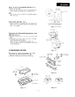
Page 38: ...1 I r 3 Through hole where front and back patterns are connected 4 5 I 6 7 7 9 10 1 11 ii 55 Figure 55 WIRING SIDE OF P W EJOARD 4 4 56 ...

Page 39: ......

Page 40: ... 2 2K i c4 l 5 F If II I c54 0 022 M B ML I _ D6 F 1 I 155133 r I 2 23 a ifi TO MAIN PWB P49 2 B c40 220 l 0 G H NOTES ON SCHEMATIC DIAGRAM can be found an page 41 2 I 3 4 I 5 6 7 6 9 10 I 11 I 72 I 59 Figure 59 SCHEMATIC DIAGRAM 5 5 6O Lll 3 9 H ...

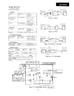
Page 41: ... M 7 0 2 PWB F 1 2 3 4 5 6 I Figure 61 CD MECHANISM EXPLODED VIEW 61 ...
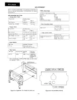
Page 42: ...A B C D I E F G H I n DECK 1 MOTOR PULLEY HEGHT 1 2 3 4 5 Figure 62 DECK MECHANISM EXPLODED VIEW l 2 6 I 62 ...

Page 43: ...1 DECK 2 E F h SOL 4 J lx 52 G H I 1 2 3 4 5 6 Figure 63 DECK MECHANISM EXPLODED VIEW 2 2 I 6 3 ...

Page 44: ...E ...

Page 45: ...G 1 J Silicon NPN 2SC3242 G 65 A B A B A A A B A B A B A B A B A B A B A A A D A B AD AC A C 4182 183 VSDTC143TS 1 J Digital NPN DTC143 T S A B 4251 VS2SC3 199GR 1 J Silicon NPN 2SC3199 GR A A 4252 VS2SB5 6 1 C 1 J Silicon PNP 2SB561 C AC Q253 VS2SC3 199GR 1 J Silicon NPN 2SC3199eGR A A 4254 VSDTC124XS 1 J Digital NPN DTC124 X S A B Q255 VS2SC3 199GR 1 J Silicon NPN 2SC3199 G R A A Q256 VS2SB5 6 1...

Page 46: ... A B A6 A B A B A B A B A B A B REF NO VRl VR2 VR251 VR481A B VR482A B VR55lA B VR700 VR710 VR750 VR751 TCl VDI x301 X651 X780 X851 XL251 PART NO DESCRIPTION CODE VARIABLE RESISTORS RVR Ml002AFZZ J 47 kohms B Semi VR A B FM Autostop Sens RVR M0997AFZZ J 5 kohms B Semi VR A B WC01 RVR M0583AFZZ J 3 3 kohms B Semi VR A B Tape Speed RVR P0167AFZZ J 100 kohm A BASS A D RVR P0167AFZZ J 100 kohm A TONE ...

Page 47: ... A A A B REF NO C262 C281 C282 C283 C284 c291 c301 C302 c303 c304 c305 c307 C308 c310 C311 312 c313 c314 c315 C316 c317 C318 321 C322 C323 C324 C325 C326 c351 354 C400A B C401 402 c403 404 C42 1 422 C423 424 C425 426 C427 C475 476 c477 C481 482 C483 484 C485 486 C487 488 C489 490 c501 c503 504 C505 506 c519 520 C521 522 C523 524 C525 526 C527 528 c529 530 C531 532 c533 534 C535 536 C537 538 c539 5...

Page 48: ...A A A A A A B A A A B A A A B A C A A A B A B A B A6 A A A B A A A A A B A A A B A B A A A B A A A B A B A A A B A B A A A B A B A A A A A A A B A B A A A B REF NO PART NO DESCRIPTION CODE C854 855 RC GZAI 06AFlC J 10 pF 16V Electrolytic A B C856 859 VCKYTVlHBlOPK J 0 001 pF 50V A A caa3 VCKYTVlEF104Z J 0 1 pF 25V A A C884 RC GZA107AFlA J 100 pF lOV Electrolytic A B C886 RC GZA107AF 1A J 100 pF lO...

Page 49: ...A A A A A A A A A A A A A A A A A A A A A A A A A A A A A A A A A A A A A A A A A REF NO R271 R272 R273 R274 R275 278 R279 R281 R282 R283 R284 R285 R286 R287 288 R292 R301 R302 R303 R304 R305 R306 R309 310 R311 R312 R313 314 R315 R316 R317 R318 R319 R320 R321 AR322 R323 AR324 R325 R326 R327 R328 R329 R330 R331 R332 R333 R334 R335 R336 R401 R402 R403 404 R405 406 R407 408 R409 410 R411 412 R413 R41...

Page 50: ...A A A A A A A A A A A A A A A A A A A A A A A A A A A A A A A A A A A A A A A A A A A A A A A A A A A A A A A A A A A A A A A A A A A A A A A A A A A A A A REF NO R706 R707 R710 R711 R712 R713 R714 R715 R716 R718 719 R720 721 R722 723 R724 R725 R732 R741 R742 R743 R745 R749 R751 R752 R753 R754 R756 R757 R758 R759 R760 R761 R762 R763 R764 R765 R766 R767 R768 R769 R770 R771 R772 R773 R774 R776 R777 ...

Page 51: ...4R99991817 J Screw Head 94R18650961 J Spacer Head SwitchSlide T y p e TIMER A 0 AECI SwitchSlide Type A D NCM705KAFZZ J Plu lOPin A C QCNCM846PAFZZ J Plug l4Pin A C QCNCM8630AFZZ J PlugPPin QCNCW623NAFZZ J Socket l3Pin W i r e Trap1 ii QCNCW620RAFZZ J Socket l6Pin A E QCNCM687FAFZZ J Plug 6Pin A B 94R18650249 J tiire Holder 94R18800201 J Head Panel 94R188002501 J Head Panel Ass y REVERSE Switch Le...

Page 52: ...Fuse Holder A A 245 QCNWNS 104AFZZ J Connector Ass y l8P1n A G 246 QCNWNS 1llAFZZ J Antenna Wire A B 247 M L I FPOOBZAFZZ J DamoerCD A F 248 HPNLH1377AFSA J Panei Cassette H o l d e r A E i COVW 249 250 255 256 257 258 259 260 261 262 263 LHLDW1068AFZZ J Nvlon Band lOOmm LHLDW1075AFZZ J N n Band 60mm PCsVP92 1OAFZZ J Cover Port GFTATlllOAFSA J L d CD HPNLH1379AFSA J Pan CD L i d JKNBZ 1283AFSA J B...

Reviews: