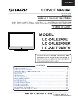

SERVICE MANUAL
Parts marked with "
" are important for maintaining the safety of the set. Be sure to replace these parts with specified ones for maintaining the
safety and performance of the set.
This document has been published to be used for
after sales service only.
The contents are subject to change without notice.
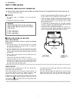
SAFETY PRECAUTION
IMPORTANT SERVICE SAFETY PRE-
CAUTION ............................................................i
Precautions for using lead-free solder ...............ii
End of life disposal ............................................ iii
CHAPTER 1. OPERATION MANUAL
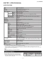
[1] SPECIFICATIONS ......................................... 1-1
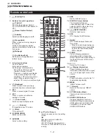
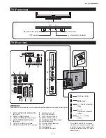
[2] OPERATION
MANUAL .................................. 1-2
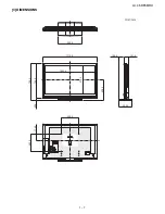
[3] DIMENSIONS ................................................ 1-7
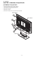
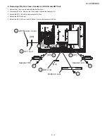
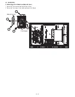
CHAPTER 2. REMOVING OF MAJOR PARTS
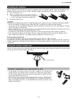
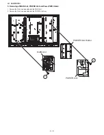
[1] REMOVING OF MAJOR PARTS ................... 2-1
CHAPTER 3. ADJUSTMENT PROCEDURE
[1] ADJUSTMENT
PROCEDURE ....................... 3-1
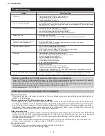
CHAPTER 4. TROUBLESHOOTING TABLE
[1] TROUBLESHOOTING
TABLE....................... 4-1
[2] LED flashing specification at the time of the
error.............................................................. 4-13
CHAPTER 5. BLOCK DIAGRAM/WIRING DIAGRAM
[1] MAIN BLOCK DIAGRAM...............................5-1
[2] SYSTEM BLOCK DIAGRAM.........................5-3
[3] OVERALL WIRING DIAGRAM......................5-4
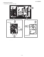
CHAPTER 6. PRINTED WIRING BOARD
[1] MAIN UNIT PRINTED WIRING BOARD........6-1
[2] LED UNIT PRINTED WIRING BOARD .........6-5
[3] KEY UNIT PRINTED WIRING BOARD .........6-6
CHAPTER 7. SCHEMATIC DIAGRAM
[1] DESCRIPTION OF SCHEMATIC DIA-
GRAM............................................................7-1
[2] SCHEMATIC
DIAGRAM ................................7-2
Parts Guide
TopPage
CONTENTS
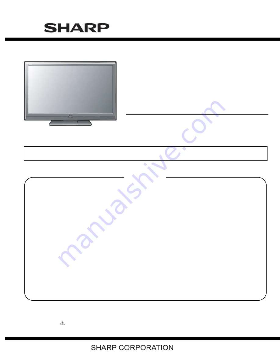
No. S08R9LC46D65E
LCD COLOUR TELEVISION
MODELS
LC-46D65E/RU
In the interests of user-safety (Required by safety regulations in some countries) the set should be restored to its orig-
inal condition and only parts identical to those specified should be used.
LC
-
46D65E/RU
Summary of Contents for Aquos LC-42DH77E
Page 50: ...LC 46D65E RU 4 16 M E M O ...
Page 80: ...LC 46D65E RU 7 20 M E M O ...