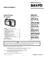
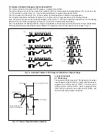
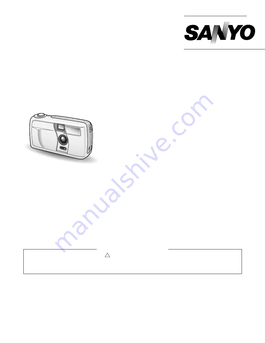
SERVICE MANUAL
Digital Camera
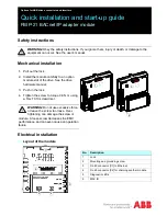
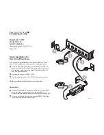
AC adaptor
VPC-R1
VPC-R1EX
(Product Code : 126 293 00)
(U.S.A., Canada)
(Product Code : 126 293 02)
(Europe, PAL General)
Contents
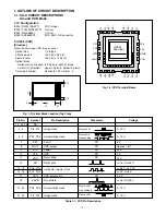
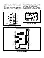
1. OUTLINE OF CIRCUIT DESCRIPTION .................... 2
2. DISASSEMBLY ........................................................ 11
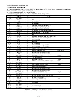
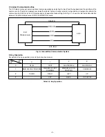
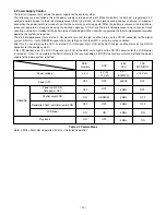
3. ELECTRICAL ADJUSTMENT .................................. 13
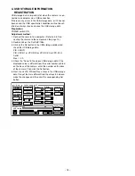
4. USB STORAGE INFORMATION
REGISTRATION ...................................................... 18
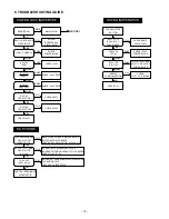
5. TROUBLESHOOTING GUIDE ................................. 19
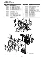
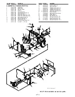
6. PARTS LIST ............................................................. 20
CABINET AND CHASSIS PARTS 1 ........................ 20
CABINET AND CHASSIS PARTS 2 ........................ 21
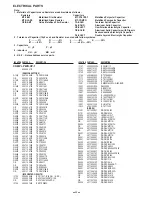
ELECTRICAL PARTS .............................................. 22
ACCESSORIES & PACKING MATERIALS ............. 26
AC Adaptor .............................................................. 26
CIRCUIT DIAGRAMS &
PRINTED WIRING BOARDS ...................................... C1
The components designated by a symbol ( ! ) in this schematic diagram designates components whose value are of
special significance to product safety. Should any component designated by a symbol need to be replaced, use only the part
designated in the Parts List. Do not deviate from the resistance, wattage, and voltage ratings shown.
CAUTION : Danger of explosion if battery is incorrectly replaced.
Replace only with the same or equivalent type recommended by the manufacturer.
Discard used batteries according to the manufacturer’s instructions.
NOTE : 1. Parts order must contain model number, part number, and description.
2. Substitute parts may be supplied as the service parts.
3. N. S. P. : Not available as service parts.
Design and specification are subject to change without notice.
SB117/U, E, EX, EX2, SVA01/U, EX, E
REFERENCE No. SM5310265
FILE NO.
PRODUCT SAFETY NOTICE
VPC-R1E
(Product Code : 126 293 01)
(U.K.)
VPC-R1G
(Product Code : 126 293 06)
(No Tax)
VAR-G5U
(Product Code : 126 301 01)
(U.S.A., Canada)
VAR-G5EX
(Product Code : 126 301 02)
(Europe, PAL General)
VAR-G5E
(Product Code : 126 301 03)
(U.K.)