Multimedia Projector
SERVICE MANUAL
PRODUCT CODE
1 122 347 00
(KJ6A)
1 122 348 00
(LJ6A)
1 122 348 02
(LJ6C)
Original Version
REFERENCE NO.
SM
5110774-00
FILE NO.
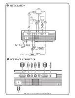
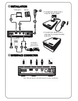
Model No. PLC-EF60A
U.S.A., Canada,
Europe, Asia, Africa
Chassis No. KJ6-EF60A00
NOTE:
Match the Chassis No. on the unit’s
back cover with the Chassis No. in the
Service Manual.
If the Original Version Service
Manual Chassis No. does not
match the unit’s
, additional Service
Literature is required. You must refer
to “Notices” to the Original Service
Manual prior to servicing the unit.
* Projection lens is optional.
Summary of Contents for PLC-EF60A
Page 102: ... 102 IC Block Diagrams TC4052BFT Selector IC9005 TC90A69F PAL Y C Separator IC2101 ...
Page 103: ... 103 IC Block Diagrams TE7780 I O Expander IC4801 IC4802 MAS1390 G Sensor IC5711 ...
Page 104: ... 104 IC Block Diagrams ...
Page 153: ...KJ6 EF60A00 153 Mechanical Parts List L15 R G Optical Filter WV Optical Filter WV S05 S05 ...
Page 154: ...KJ6 EF60A00 154 Mechanical Parts List 1 2 0 5 L03 Integrator In Integrator In ...
Page 156: ...KJ6 EF60A00 156 Mechanical Parts List L09 Mirror R Mirror R S05 S05 ...
Page 157: ...KJ6 EF60A00 157 Mechanical Parts List 157 Relay lens Out L08 Relay Lens Out ...
Page 160: ... KJ6A Feb 2006 BB 400 Printed in Japan SANYO Electric Co Ltd ...
Page 184: ...Diagrams Drawings KJ6 EF60A00 ...