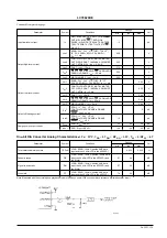
background image

Overview

The LC78626KE is a monolithic compact disk player
signal processing and servo control CMOS IC equipped
with an internal anti-shock control function. Designed for
total functionality including support for EFM-PLL, and
one-bit D/A converter, and containing analog low-pass
filter, the LC78626KE provides optimal cost-performance
for low-end CD players that provide anti-shock systems
by eliminating as many unnecessary features as possible.
The basic functions provided by this IC include
modulation of the EFM signal from the optical pick-up,
deinterleaving, detection and correction of signal errors,
prevention of a maximum of approximately 38 seconds of
skipping, signal processing such as digital filtering (which
is useful in reducing the cost of the player), and processing
of a variety of servo-related commands from the
microprocessor. The LC78626KE is an improved version
of the LC78626E. It provides 8

×

oversampling digital

filters and supports up to 16M of DRAM.

Functions

• When an HF signal is input, it is sliced to precise levels

and converted to an EFM signal. The phase is compared
with the internal VCO and a PLL clock is reproduced at
an average frequency of 4.3218 MHz.

• Precise timing for a variety of required internal timing

needs (including the generation of the reference clock) is
produced by the attachment of an external 16.9344 MHz
crystal oscillator.

• The speed of revolution of the disk motor is controlled

by the frame phase difference signal generated by the
playback clock and the reference clock.

• The frame synchronizing signal is detected, stored, and

interpolated to insure stable data read back.

• The EFM signal is demodulated and converted to 8-bit

symbolic data.

• The demodulated EFM signal is divided into subcodes

and output to the external microprocessor. (Three
general I/O ports are shared [exclusively] for this
purpose.)

• After the subcode Q signal passes the CRC check, it is

output to the microprocessor through a serial
transmission (LSB first).

• The demodulated EFM signal is buffered in the internal

RAM, which is able to absorb ±4 frame’s worth of jitter
resulting from variations in the disk rotation speed.

• The demodulated EFM signal is unscrambled to a

specific sequence, and deinterleaving is performed.
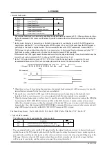
Package Dimensions

unit: mm

3151-QFP100E 

21.6

0.8

3.0max

1.6

17.2

0.825

1

30

31

50

51

80

81

1.6

0.575

0.575

0.15

2.7

15.6

0.3

20.0

23.2

14.0

0.65

0.825

100

0.8

0.65

0.1

CMOS IC

21099RM(OT) No. 5995-1/34

SANYO: QFP100E (QIP100E)

[LC78626KE]

SANYO Electric Co.,Ltd. Semiconductor Bussiness Headquarters

TOKYO OFFICE Tokyo Bldg., 1-10, 1 Chome, Ueno, Taito-ku, TOKYO, 110-0005 JAPAN

DSP for Compact Disk Players

LC78626KE

Ordering number : EN5995

Continued on next page.

Any and all SANYO products described or contained herein do not have specifications that can handle
applications that require extremely high levels of reliability, such as life-support systems, aircraft’s
control systems, or other applications whose failure can be reasonably expected to result in serious
physical and/or material damage. Consult with your SANYO representative nearest you before using
any SANYO products described or contained herein in such applications.

SANYO assumes no responsibility for equipment failures that result from using products at values that
exceed, even momentarily, rated values (such as maximum ratings, operating condition ranges, or other
parameters) listed in products specifications of any and all SANYO products described or contained
herein.

Summary of Contents for LC78626KE

Page 1: ... signal is demodulated and converted to 8 bit symbolic data The demodulated EFM signal is divided into subcodes and output to the external microprocessor Three general I O ports are shared exclusively for this purpose After the subcode Q signal passes the CRC check it is output to the microprocessor through a serial transmission LSB first The demodulated EFM signal is buffered in the internal RAM ...

Page 2: ... The digital output is equipped internally High speed access is supported through discretionary track counting Using the 8 oversampling digital filter D A converter signals with improved continuity of output data are produced A type D A converter using a 3 order noise shaper is equipped internally An analog low pass filter is equipped internally Internal digital attenuator 8 bit α 239 steps Intern...

Page 3: ...tor 4 oversampling digital filter C1 C2 error detection and correction flag process VCO clock production clock control Slice level control Sync detect EFM demodulation CLV digital servo Subcode partition QCRC Microprocessor interface Servo commands General ports Disable Crystal oscillator system timing generator One bit DAC Low pass filter ADPCM decoder DRAM control Overflow process initiation con...

Page 4: ...es 1 to 3 400 ns Low level clock pulse width tWL SBCK CQCK Figures 1 to 3 400 ns Data read access time tRAC SQOUT PW Figures 2 and 3 0 400 ns Command transfer time tRWC RWC Figure 1 1000 ns Subcode Q read enable time tSQE WRQ Figure 2 no RWC signal 11 2 ms Subcode ready cycle time tSC SFSY Figure 3 136 µs Subcode read enable time tSE SFSY Figure 3 400 ns Port input data setup time tCSU CONT2 to CO...

Page 5: ... 0 44 V DRAM3 to DRAM0 IOL 0 5 mA VOL5 MMC0 to MMC3 IOL 2 mA 0 96 V PDO CLV CLV JP JP IOFF1 CONT2 to CONT5 DRAM0 to DRAM3 5 µA Output off leakage current ASRES VOUT VDD PDO CLV CLV JP JP IOFF2 CONT2 to CONT5 DRAM0 to DRAM3 5 µA ASRES VOUT 0 V Charge pump output current IPDOH PDO RISET 68 kΩ 30 42 54 µA IPDOL PDO RISET 68 kΩ 54 42 30 µA Parameter Symbol Conditions Ratings Unit min typ max Total har...

Page 6: ...Figure 1 Command Input Figure 2 Subcode Q Output Figure 3 Subcode Output No 5995 6 34 LC78626KE ...

Page 7: ...No 5995 7 34 LC78626KE Figure 4 General Port Input Timing Figure 5 General Port Output Timing ...

Page 8: ...utput 23 HFL I Track detect signal input Schmidt input 24 TES I Tracking error signal input Schmidt input 25 TOFF O Tracking off output High level output 26 TGL O Tracking gain switch output Gain is increased with low level Undefined 27 JP O Track jump control output Can be 3 state output depending on the command Low level output 28 JP O 29 PCK O EFM data playback clock monitor 4 3218 MHz during p...

Page 9: ...r supply 59 XOUT O 16 9344 MHz crystal oscillator connection 60 XIN I 61 XVSS P Crystal oscillator ground Must be connected to 0 V 62 RWC I Read write control input Schmidt input 63 COIN I Microcontroller command input 64 CQCK I Input pin for the command input latch clock and the subcode readout clock Schmitt input 65 SQOUT O Subcode Q output Undefined 66 WRQ O Subcode Q output standby output Unde...

Page 10: ...ata bus Input mode 82 DRAM2 I O DRAM data bus Input mode 83 DRAM1 I O DRAM data bus Input mode 84 DRAM0 I O DRAM data bus Input mode 85 OE O DRAM control signal Low level output 86 WE O DRAM control signal High level output 87 CAS O DRAM control signal Undefined 88 RAS O DRAM control signal Undefined 89 AD9 O DRAM address bus Low level output 90 AD8 O DRAM address bus Low level output 91 AD7 O DRA...

Page 11: ...k Circuit Pin 3 PDO Pin 5 ISET and Pin 7 FR The VCO circuit is equipped internally and the PLL circuit is structured using external resistors and external capacitors The ISET is the reference current for the charge pump The PDO is the loop filter for the VCO circuit and the FR is the resistor that determines the frequency range of the VCO Reference Values R1 68 kΩ C1 0 1 µF standard speed C1 0 047...

Page 12: ...et of RWC General port I O settings Single byte commands Two byte commands RWC 2 set for the track count Two byte commands RWC 1 set digital attenuation and setting the general I O port Eliminating command noise This command makes it possible to reduce the noise that is mixed into the CQCK clock This is effective for noise of less than 500 ns however the CQCK timing must be set to have 1 µs or mor...

Page 13: ...ective forms on control when the internal modes of the DSP change The PWM frequency is 7 35 kHz The V P has a high output when the internal mode is the rough servo and a low output when the internal mode is phase control Switching the rough servo gain When the internal mode is the rough servo the CLV control gain for the 8 cm disk can be reduced by 8 5 dB from the level for the 12 cm disk No 5995 ...

Page 14: ...ill cause the spindle gain to fall by 6 dB it will be necessary to increase the gain on the servo side No 5995 14 34 LC78626KE Code COMMAND RES low B1 CLV phase comparator 1 2 frequency division B2 CLV phase comparator 1 4 frequency division B3 CLV phase comparator 1 8 frequency division B0 CLV phase comparator no frequency division Code COMMAND RES low B4 CLV 3 state output B5 CLV 2 state output ...

Page 15: ...s processes etc use in conjunction with the microcontroller is recommended When the internal brake mode is in effect then it is possible to monitor the disk deceleration status at the WRQ Pin by executing the DISC MTR BRAKE command 06 in this DSP However if another command is executed while this command is in process then the command will be aborted When you wish to prevent the function from being...

Page 16: ...ted to the disk control mode and this terminal is high during start stop and break control Moreover the TOFF pin can be turned on and off independently using commands However the disk motor control is only enabled when the CLV mode is active No 5995 16 34 LC78626KE Code COMMAND RES low A0 The conventional track jump A1 The new track jump 11 1 TRACK JUMP IN 1 12 1 TRACK JUMP IN 2 31 1 TRACk JUMP IN...

Page 17: ...in the conventional mode 1 TRACK JUMP IN OUT 2 0 5 TRACK 233 µs 60 ms 0 5 TRACK The same 60 ms JUMP period JUMP period as for a 1 TRACK JUMP IN OUT 3 0 5 TRACK 233 µs This period 0 5 TRACK The same This period JUMP period does not exist JUMP period as for a does not exist 1 TRACK JUMP IN OUT 4 0 5 TRACK 233 µs 60 ms TOFF L 0 5 TRACK The same 60 ms TOFF L JUMP period during period C JUMP period as ...

Page 18: ...d with a single pin however the gain must be increased on the servo side because the kick gain will decrease by 6 dB Track check mode After the track check IN or track check OUT command has been entered then when a discretionary number between 8 and 254 is entered as binary data a track count of the specified number 1 will be performed No 5995 18 34 LC78626KE Code COMMAND RES low B6 JP 3 state out...

Page 19: ...created by frequency dividing the crystal clock For each frame the error correction status is output to EFLG It is easy to tell the quality of the playback by the number of high pulses that appear in the EFLG signal The Subcode P Q and R to W Output Circuits Pin 34 SBCK Pin 35 SFSY CONT4 Pin 36 PW CONT5 Pin 37 SBSY PW is the subcode signal output pin Note Pin 35 and Pin 36 are respectively a gener...

Page 20: ...ta updating At this time WRQ goes low Because WRQ goes low after being high for 11 2 ms the CQCK input starts during the interval when WRQ is high The data can be read beginning with the least significant bit Note 1 This conditions is ignored if an address free command is sent corresponding to the CDV The items within the parentheses are for the read in area The WRQ pin normally indicates the subc...

Page 21: ...e set to a range from 00H to EEH 239 different levels by the microcontroller commands This two byte command is different from the two byte commands used in track counting in that RWC only needs to be set once and it is not necessary to reset the two byte command either See the two byte command RWC1 set on page 13 After inputting the target attenuation level in terms of 00H to EEH then if the atten...

Page 22: ...in is equipped with an internal driver it can drive a transformer directly The digital OUT pin can be fixed low by inputting the DOUT OFF command Of the DOUT data the UBIT data can be fixed at low by entering the UBIT OFF command By entering the CDROM XA command the DOUT pin can be switched to CD ROM data that is not subjected to interpolation or to mute control When this is done the audio output ...

Page 23: ...t sequentially from CONT2 CONT3 CONT4 and CONT5 with the falling edge of the CQCK from the SQOUT pin when there is a port read command The command uses a single byte command format When a command is applied to this DSP during a track check track jump or internal MTR brake operation then the DSP will terminate those operations If you do not wish to terminate these operations do not apply unnecessar...

Page 24: ...ing the double speed playback command Recommended crystal ceramic oscillator constants The load capacitance Cin and Cout will have different requirements depending on the actual print circuit board used and thus it is necessary to perform verification testing on the use print circuit board Consult the oscillator manufacturer 16M and 4 2M Pins Pin 41 16M Pin 42 4 2M When using double speed normal s...

Page 25: ...s buffer margin is checked and by precisely controlling the CLV servo circuit PCK side frequency ratio it is possible to control the data write address so that it will be centered on the size of the buffer Also when the 4 frame buffer capacity is exceeded the write address can be forced to 0 and because the resulting errors cannot be subjected to flag processing the mute is applied for a 128 frame...

Page 26: ... Depending on the DRAM capacity 1M 4M 8M 16M bits the time that can be stored will be approximately 2 4 seconds 1M approximately 9 5 seconds 4M approximately 19 seconds 8M or approximately 38 seconds 16M Depending on the type of DRAM the MR1 MR2 might have to be set See the table When in the anti shock mode the double speed data is written to the external DRAM and then read at normal speed 1 speed...

Page 27: ...sed by setting this pin high Furthermore when controlling the independent reset using commands the ASRES pin must be tied low connected to 0 V No 5995 27 34 LC78626KE Code COMMAND RES low F4 Independent reset disable release F5 Independent reset enable inrush Beginning of L point search L point is found Beginning of writing to the DRAM L point because of shock Track jump L point because the DRAM i...

Page 28: ...BIT ON 60 01 MUTE 0 dB 21 TJ time TOFF H 41 UBIT OFF 61 02 22 New Track Count 42 DOUT ON 62 03 MUTE dB 23 Old Track Count 43 DOUT OFF 63 04 DISC MTR START 24 44 64 05 DISC MTR CLV 25 45 65 06 DISC MTR BRAKE 26 46 66 07 DISC MTR STOP 27 47 67 08 FOCUS START 1 28 STO CONT 48 68 09 ADDRESS FREE 29 LCH CONT 49 69 0A 2A RCH CONT 4A 6A 0B 2B 4B 6B 0C 2C 4C 6C 0D 2D 4D 6D 0E 2E 4E 6E DF normal speed OFF ...

Page 29: ... 89 ADDRESS 1 A9 DISC 12 cm SET C9 E9 8A AA CA Internal BRK DMC L EA 8B ROMXA RST AB CB Internal BRK DMC H EB 8C TRACK JMP BRAKE AC PLL DIV OFF CC Internal BRK time TOFF EC 8D OSC OFF AD PLL DIV ON CD Internal BRK time TON ED 8E OSC ON AE CE X tal 16M EE Command noise OFF 8F TRACKING ON AF CF EF Command noise ON 90 F OFF ADJ START B0 CLV PH1 frequency divider mode D0 F0 TRACK CHECK 2BYTE DETECT 91...

Page 30: ...Sample Application Circuit No 5995 30 34 LC78626KE ...

Page 31: ...al is necessary Also the same potential must be supplied to all supply voltage pins on the ASP IC Do not allow the pin voltages on any of the input or output pins to exceed VDD or to fall lower than VSS The timing of signal application requires special care at power on to assure that this condition is met Do not allow overvoltages or abnormal noise to be applied to this IC In general latch up can ...

Page 32: ... 4 2MHz output is used as the microcontroller master clock the reset circuit will be shared with the microcontroller Since the microcontroller will not be reset unless a clock signal is applied do not control the reset input to this IC from a microcontroller output port If this IC has not been reset the 4 2 MHz output is not guaranteed and the microcontroller may not be reset This can result in in...

Page 33: ...utputs are used issue a UBIT OFF 41 command to this IC during initialization UBIT ON 40 should only be used during playback to prevent DIR unlock and incorrect subcode recognition During initialization after clearing an IC reset and after turning this IC s oscillator on issue a 2 byte reset command FF to the LA9230M Series or LA9240M Series ASP to set up the ASP command register Since the LA9230M ...

Page 34: ...ur Such measures include but are not limited to protective circuits and error prevention circuits for safe design redundant design and structural design In the event that any or all SANYO products including technical data services described or contained herein are controlled under any of applicable local export control laws and regulations such products must not be exported without obtaining the e...

Reviews: