Specifications
POWER RATING . . . . . . . . . . . . . . . . . . . . . . . . . 120VAC
162 W (AVG.)
ANTENNA INPUT IMPEDANCE. . . . . . . . . . . . . . . . . 75
Ω
UHF/VHF/CATV
DIGITAL
RECEIVING CHANNEL . . . . . . . . . . . . . . . . . 2 - 13 (VHF),
14 - 69 (UHF),
01, 14-94, 95-135 (CATV)
1-135 (DIGITAL)
REMOTE READY. . . . . . . . . 36 KEY REMOTE CONTROL
SOUND OUTPUT. . . . . . . . . . . . . . . . . . . . . . . 10.0 W/CH
INTERMEDIATE FREQUENCY
PICTURE IF CARRIER . . . . . . . . . . . . . . . . . . 45.75MHz
SOUND IF CARRIER . . . . . . . . . . . . . . . . . . . 41.25MHz
COLOR SUB CARRIER . . . . . . . . . . . . . . . . . 42.17MHz
CABINET DIMENSIONS
WIDTH . . . . . . . . . . . . . . . . . . . . . . . . . . . . . . . 1055mm
HEIGHT . . . . . . . . . . . . . . . . . . . . . . . . . . . . . . . 723mm
DEPTH INCLUDING BASE . . . . . . . . . . . . . . . . 246mm
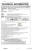
REFERENCE No.
SM
780190
DP42740, J4HG, PRODUCT CODE 111011104
FILE NO.
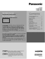
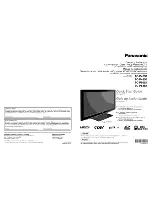
SERVICE MANUAL
Remote Control Digital
Color Television
DP42740
(U.S.A.)
(CANADA)
ORIGINAL VERSION
Chassis No. P42740-04
NOTE:
Match the Chassis No. on
the unit’s back cover with
the Chassis No. in the
Service Manual.
If the Original Version
Service Manual Chassis
No. does not match the
unit’s,
additional Service
Literature is required. You
must
refer to “Notices” to the
Original Service Manual
prior to servicing the unit.
POWER MENU ENTER
VOL
CH
Servicing should be performed by only trained and qualified service personnel.
Contents
SAFETY INSTRUCTIONS. . . . . . . . . . . . . . . . . . . . . . . . . 2
SERVICE ADJUSTMENTS . . . . . . . . . . . . . . . . . . . . . . . . 3
ON-SCREEN SERVICE MENU . . . . . . . . . . . . . . . . . . . . . 4
POWER FAILURE CIRCUIT . . . . . . . . . . . . . . . . . . . . . . . 5
MECHANICAL DISASSEMBLY . . . . . . . . . . . . . . . . . . . . 6
CHASSIS ELECTRICAL PARTS LIST . . . . . . . . . . . . . . . . 8
COMPONENT AND TEST POINT LOCATIONS . . . . . . 20
BLOCK DIAGRAM POWER LINES. . . . . . . . . . . . . . . . . 23
BLOCK DIAGRAM SIGNAL LINES . . . . . . . . . . . . . . . . 24
IC BLOCK DIAGRAMS . . . . . . . . . . . . . . . . . . . . . . . . . . 25
TROUBLESHOOTING FLOW CHARTS . . . . . . . . . . . . . 31
MAIN IC(SIGNAL PROCESSOR) & PERIPHERICALS . . 34
SCHEMATIC NOTES . . . . . . . . . . . . . . . . . . . . . . . . . . . 35
IC, DIODE, AND TRANSISTOR PIN LAYOUTS. . . . . . . 36
PC BOARD CONNECTIONS AND LOCATIONS . . . . . . 37
CAPACITOR AND RESISTOR CODE CHART . . . . . . . . 38
SCHEMATIC DIAGRAMS. . . . . . . . . . . . . . . . . . . . . . . . 39
© Sanyo Manufacturing Corporation 2011
Summary of Contents for DP42740 - 42"Class 720p Plasma
Page 25: ... 25 IC BLOCK DIAGRAMS IC001 Audio AMP ...
Page 26: ... 26 IC1600 IC1640 DC to DC Converter IC BLOCK DIAGRAMS CONT IC1620 DC DC converter ...
Page 27: ... 27 IC5650 IC5660 IC5900 Voltage detector IC5750 Flash Memory ...
Page 29: ... 29 IC6250 Voltage comparator IC5700 DDR Double Data Rate SDRAM ...
Page 30: ... 30 IC BLOCK DIAGRAMS CONT IC6500 IC6530 IC6560 Logic AND gate IC 6600 USB Protection ...