background image

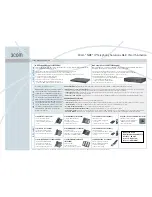
Summary of Contents for CLT-136

Page 1: ...0 ch 16 digits 10 ch auto scan 65 536 random 3 weeks yes yes yes yes yes Specifications subject to change without notice Cordless Telephone CLT I 36 NZ 1 CLT I 36 WH NZ Tone Pulse Antenna Power Source Base station Handset Dimensions Base station Handset Accessories PRODUCT CODE No 163058 97 BLACK 163058 94 WHITE yes Rod Base Station Rubber Handset AC adaptor AC 230 240V 50Hz DC9V Ni Cd battery 3 6...

Page 2: ...OPERATION c v w v 1 ...

Page 3: ...should not be placed near or on top of a TV or VCR and if interference is experienced moving the cordless telephone farther away from the TV or VCR will often reduce or 1 eliminate the interference INITIAL HANDSET BATTERY CHARGE Install the handset battery supplied in the handset and charge the handset for a full 12 hours before using the cordless phone for the first time IMPORTANT Never attempt t...

Page 4: ...vailable to transmit signals between the base station and handset If you notice interference durina a call simcrlv mess the CAUTION This telephone is for use tone dialing system only If you have a pulse dialing line you can t use this cordless telephone SECURITY CODES Your cordless telephone works only when the same security code is selected from 65 536 possibilities for both the handset and base ...

Page 5: ... cord NOTE t DC 9V jack TEL LINE jack USE ONLY SANYO AC ADAPTOR MODEL NO KR0522 APPROVAL NO Q921 03 ANSWERING A CALL When a call comes in the TALK indicator flashes 1 Press or Lift the handset from the base station ANY KEY ANSWER You can also answer a call by pressing any key except 2 Talk 3 Press to hang up NOTE I If the handset is too far awa from the d base station pressing END may not o TALK o...

Page 6: ...ll is placed on hold and you can talk to the second caller Press Im again The second caller is dated on hold and NOTE The button may also be used to get a new dial tone without pressing or replacing the handset in the base station cradle However if your telephone line has special service features like call waiting the button may not operate in this way PAG13FIND BUTTON you can talk to the first ca...

Page 7: ...OITOM CABINET AND ANTENNA b REMOVAL OF ANTENNA AND MAIN P C BOARD 1 Remove three of screw 1 from the bottom cabinet 1 After removing screw 1 it removes Lug 2 and an antenna 3 2 Remove the bottom cabinet 2 2 After removing two of screw 4 it removes a SW P C board 5 3 After removing two of screw 6 it removes a Main P C board 7 5 44 1 Ii 1 6 ...

Page 8: ...ea to release the hooks on both sides of the cabinet 4 gently open the bottom of the cabinet 5 While gently opening the handle lift and remove 6 and 7 Push Push Press b 1 2 c 1 2 2 REMOVAL OF MAIN P C BOARD Remove the solder between the antenna lead pin and the Main P C board Remove the six of screw 1 to remove the Main P C board 2 I Unsolders I REMOVAL OF ANTENNA Remove the DEC window 1 Remove th...

Page 9: ...nect theantenna wire from the set For test mode condition please refer to Remarks PARTS LOCATION a VR351 j VR651 T351H CT151 T253 T152 j T251 fi TEST POINT LOCATION MIC IN H M C IN E sP ouT a vco E ANT OPEN ANT IN H dCC B SP OtiT H TX VCO H R VCO H AN IN E 8 ...

Page 10: ... 3 TABLE 3 Test Equipment RF Electronic Voltmeter Frequency Counter Linear Detector AF Oscillator Dummy Load 50s2 Unit Condition a From the mode mentioned in 1 1 change toTEST CH 4 by pushing 4 x key b Disconnect frequency counter and connect RF electronic voltmeter to ANT 1 and 2 pin 50Q probe c Tx POWER d Tx FREQUENCY e Tx MODULATION Align T251 to obtain 8 0A 3 0 dBm from read of RF voltmeter Co...

Page 11: ...8 OdBm A 3dB 2 Tx FREQUENCY FREQ side CT151 39 925 MHz 39 925MHz 0 5kHz Adjustment T 2 Output Impedance 600Q AF Oscillator L TABLE 2 Unit MIC ANT H Linear Detector MIC ANT E FIG 3 STEP CONDITION ADJUST ADJUSTED VALUE SPECIFICATION 3 MIC Mod OSC OUTPUT 1kHz VR651 1 5kHz dev 1 5 f 0 1 kHz dev at 7th 1OmV 300Hz 1 4 t 0 3kHz dev 3kHz 2 35 0 5kHz dev w 4 DATA Mod 4 OkHz dev 4 0 K v at 7kHz TABLE 3 1o ...

Page 12: ... voltmeter and distortion meter respectively Rx RF Reduce output level of FM SSG from 46dBp to 5dBp Align T151 to obtain minimum distortion at the distortion meter less than 10 0 AF LEVEL Change output level of FM SSG from 5dBp to 46dBp Align VR351 to obtain 50mV A 5mV from read of AF voltmeter and confirm at the FM SSG input of 300Hz the output of AFVM 60mV k 3dB 3kHz the output of AFVM 10mV 3dB ...

Page 13: ...ect the antenna wire from the set For test mode condition please refer to Remarks PARTS LOCATION CT101 VR601 I TEST POINT LOCATION kR302 T301 T202 wr301 TIOI CNIO1 CN90 RF IN E RF IN H I 220p lov m RX VCO TX VCO AUTO SCAN Q Clll side C213 side C D 12 ...

Page 14: ...1 Select channel 10 by pushing PAGE key Connect digital voltmeter to TtiRx VCO TEST POINT Align T201 Tx and TI 02 Rx to obtain 2 5V 0 1 V DC from read of digital voltmeter respectively Adjustment Unit 1 1 Iclol pi T Vco TX C215 SIDE Frequency CN101 H b 3 pin Rx VCO o Digital Counter Voltmeter CN101 E Rx GND C101 SIDE FIG 1 STEP CONDITION ADJUST ADJUSTED VALUE SPECIFICATION 1 Tx VCO Tx VCO side T20...

Page 15: ...near detector to CN1 01 Connect AF oscillator 1kHz 20dBm to TEL line Align VR601 to obtain 2 OkHz f O 1kHz dev from the read of linear detector And confirm at the AF oscillator to TEL line 300 Hz 20dBm the read of linear detector 1 4kHz f 0 3kHz dev 3 kHz 20dBm the read of linear detector 3 OkHz f 0 5kHz dev Tx DATA MODULATION After Tx modulation alignment disconnect DC 9V from the unit and open 1...

Page 16: ...d connect AF voltmeter in Disconnect Linear detector from CN101 and connect FM SSG 1kHz 2 5kHz dev 39 9000MHz 46dBp to CN1 01 EWE EbLBE N I EVEL Align T301 to obtain maximum deflection and minimum distortion from the read of AC voltmeter and distortion meter respectively Change output level of FM SSG from 46dBp to 12dBp Align T101 to obtain minimum distortion at the distortion meter less than 107 ...

Page 17: ...o TX FREQ RX FREQ RX LOCALFREQ TX FREQ RX FREQ RX LOCALFREQ 30 075 MHz 39 775 MHz 29 080 MHz 30 100 MHz 39 800 MHz 39 775 MHz 30 075 MHz 19 380 MHz 2 29 105 MHz A 39 800 MHz 30 125 MHz 39 825 MHz 30 100 MHz 19 405 MHz 29 130 MHz 2 7 30 150 MHz 39 825 MHz 39 850 MHz 30 125 MHz 19 430 MHz 29 155 MHz 7 3 30 175 MHz 39 850 MHz 30 150 MHz 19 455 MHz 39 875 MHz 29 180 MHz 3 30 200 MHz 39 875 MHz 30 175 ...

Page 18: ...TMENT mode ON OFF ON OFF 10 1 and 6 TX ADJUSTMENT mode ON OFF ON ON 7 1 and 9 RX ADJUSTMENT mode ON ON ON OFF 2 1 and At aforementioned three any mode the following item from 2 to 7 can operate it 2 3 4 5 PLL Channel setting TX POWER off 1 Setting by the numeric keys The numeric key is pressed then the TX power is turned off TX and RX channels will be set The channels range from 1ch to 10ch and ar...

Page 19: ...ICO02 3 Charge detection When CHARGE is detected the TALK LED is lit 4 Return to the usual mode By turning off the power and retry the usual mode will start 6 Ignore security code mode Through the base receiving a specific security code and channel security AC34H channel 10ch this mode allows linking of the remote and base without security registration by the remote Other operations perform as usu...

Page 20: ...y keep off Test mode will be Remote Unit Call Status In case of Test mode in this way to switchover the usual mode is either one of the following ways 1 detect charge 2 turn off the power retry 3 Types of test modes Test mode has the following 3 states Description of state is explained in below table State Name Description LED 1 Remote Unit Call IN USE 2 DTMF Output Output 1 5 9 and of DTMF repeat...

Page 21: ...tection differs by the switchover of the Test Mode and the Usual Mode 1 Switchover by operation of microcomputer port In case of the Remote Unit Call while detecting charge the CHARGE LED is set ON In case of the DTMF output and the PULSE output the CHARGE LED is always set ON 2 Switchover by operation of Power On A Charge detection switches over from the Test Mode to the Usual Mode REMARK 1 The T...

Page 22: ...EXPLODED VIEW HANDSET 207 272 3 208 201 202 251 Y203 271 Y202 t 205 21 ...

Page 23: ...EXPLODED VIEW BASE STATION 109 Ylol Jill Ylol 22 ...

Page 24: ...GE ASSY CABINET BOTTOM WHITE ASSY CABINET BOTTOM BLACK CABINET WHITE CABINET BLACK CUSHION RUBBER SPEAKER ASSY CABINET REAR WHITE ASSY CABINET REAR BLACK ASSY LID BATTERY WHITE ASSY LID BATTERY BLACK CUSHION MIC TERMINAL CHARGE L TERMINAL CHARGE R BUTTON RUBBER DIAL KEY DEC WINDOW LED FIXING PARTS REF NO PART NO Ylol 4110214005 Y201 4110228903 Y202 4110228408 Y203 4110228408 ELECTRIC PART REF NO P...

Page 25: ...624 T1 BV4 REF NO QO02 or or QO03 QO04 Qo05 or or QO06 or 151 Q152 Q153 Q251 Q252 Q253 Q651 652 or Q690 or ROO1 RO03 RO04 RO08 RO1O RO11 R012 R013 R014 R015 R016 R017 R018 R019 R020 R021 R022 R023 R024 R025 R026 R151 R152 R153 R154 R155 R156 R157 R158 R159 R160 R161 R162 R165 R166 RI 67 R168 R169 R170 R251 R252 R254 R255 R256 R257 PART NO DESCRIPTION 4050026706 TR 2SA1179 M6 TB 4050020308 TR2SA103...

Page 26: ...260 R261 R262 R263 R264 R265 R275 R276 R351 R352 R353 R354 R355 R356 R358 R650 R651 R652 R653 R654 R655 R656 R657 R659 R660 R662 R663 R664 R665 R666 R667 R668 R669 R671 R672 R673 R674 R675 R676 R677 R678 R679 R681 R690 R691 R692 R693 R694 R695 T151 T152 T251 T252 T253 T351 VR351 VR651 Xool X151 XF151 XF351 or or or XF352 REF NO PART NO 171 cl 01 cl 02 cl 03 cl 04 cl 05 Cllo Clll C112 C113 C114 C11...

Page 27: ...E GMAO1 BT DIODE 1SS133 T 77 DIODE GMAO1 BT LED BR1102W TR LED BR1 102W TR REF NO D901 or D902 or D903 or or or or or D904 or or or or or D905 or D907 D908 D909 D91O D911 D912 Iclol IC301 IC401 IC402 IC601 IC602 IC901 or or L101 L102 L901 L902 L903 L904 L905 Q101 Q201 Q202 Q204 or or Q301 or Q401 or or Q701 or Q702 or Q704 901 Q902 or Q904 905 or Q906 or Q908 R101 PART NO 4070639108 4070517505 407...

Page 28: ...A Ill OW 4010128006 CARBON lOOK JA l 4W 4010383603 MT GLAZE 3 3K JA 1 1OW 4010375707 MT GLAZE 100K JA 1 1 OW 4010375202 MT GLAZE 100 JA 1 1OW 4010379309 MT GLAZE 18K JA Ill OW 4010380800 MT GLAZE 22K JA 1 1OW 4010380800 MT GLAZE 22K JA 1 1 OW 4010380800 MT GLAZE 22K JA 1 1 OW 4010383603 MT GLAZE 3 3K JA Ill OW REF NO R614 R617 R618 R625 R630 R631 R632 R701 R702 R703 R704 R705 R706 R707 R708 R709 R...

Page 29: ...nector CNOOI Is the level of the reset terminal of pin 21 of ICOOI NO High 7 Check ICO03 I t YES Is the frequency of pin 20 of ICOO1 4 15MHz Check XOO1 and ICOO1 The security code cannot be registered Base station Voice communication are not possible by pushing by the TALK button The unit does not link Is the level of pin 29 of IC401 Low Check charger terminals Q904 I A Yts v NO Isa carrier signal...

Page 30: ...NO to the antenna IYES I Is there voltage in terminal C of Q253 ICheck QO02 ICheck ICOO1 J I I 1 I T Is RX data being input to pin 8 of ICOO1 Is RX data being input pin 9 of IC351 4 YES YES i NO Check QOO1 Check Q151 and IC351 e 1 2 3 4 5 Transmission signal IHandset I Does the transmission signal reach pin 24 of IC652 Check MIC and D670 Does the transmission signal reach pin 1 of IC653 Check IC65...

Page 31: ... the level of pin 19 of NO IC401 Hiah Check IC401 Check T901 3 I Does the voice signal reach pin 24 of IC601 I 4 5 6 YES NO Check Q704 I I YES Is the level of terminal B NO Check Q905 of Q905 High ICheck Relay I Does the voice signal reach pin 18 of IC601 Is the level of pin 17 of IC601 High YES YES NO Handset Check IC601 Check IC101 1 Does the voice level reach pin 9 of IC351 Check IC351 Q151 YES...

Page 32: ...d Base station linked ICheck refer to the section c and d I 1 YES v Does the ringer signal reach pin 1 and 2 of IC901 Check CN901 L903 L904 D903 and D904 YES Is the High Low signal being emitted to pin 3 and 4 of IC901 Check Q901 YES Is the High Low signal being emitted to pin 24 of IC401 Check Q906 I YES Handset 1 t Is the ringer tone signal being output to pin 10 of ICOO1 Check ICOO1 Is the ring...

Page 33: ... DTMF OUTPUT o 7 RX MUTE RX MUTE CONTROL L o 22 CHARGE LED CHARGE LED CONTROL L o 8 Vss POWER GND 23 TIP 9 Oscl SYSTEM CLOCK IN 4 093MHz I 24 RING RINGER SIGNAL INPUT L RING I 10 OSC2 SYSTEM CLOCK OUT 4 093MHz o 2 5 A SCAN AUTO SCAN SIGNAL LEVEL DETECT H I 11 VDD POWER VDD 26 PAGE PAGE KEY INPUT I 12 RESET SYSTEM RESET INPUT L I 27 M BIFLASH SET MAKE BREAK or FLASH I 13 TEST NO USE I 28 MIB SET MA...

Page 34: ...2 a n o J 2nd MlX lN2 OSCBUFFER OUT n 2nd MIX IN1 EMia 2nd OSCl UI M g FILTER OUT ox go gz TV 2nd OSC2 S FILTER IN 2nd MiX OUT AF OUT VCC2 SIGNAL DET IF IN SCHMllT OUT D c NOISE OET IF OUT OUAD CMP NF CMP V REC CMP OUT LPF2 IN LPF2 OUT CMP MUTE CON1 EXP MUTE CONT TX DATA IN V REF Vcc w I 1 I I 3 m N w i L g z z o 0 c c C l m m m if ...

Page 35: ...POWER CONTROL 1 L o 35 PDO NO USE 12 HOLD NO USE I 36 PD1 NO USE 13 COUNTRY SET COUNTRY US L AU H I 37 PD2 Nfl I ISF 14 RX MUTE RX MUTE CONTROL L o 38 PD3 NO USE 15 TEST NO USE 39 VDD POWER B 16 Vss POWER GND 40 CHARGE CHARGE DETECT H I 17 Oscl SYSTEM CLOCK IN I 41 PE1 Nr7 ISF I I NO USE 18 NC 19 NC NO USE 1431NU 20 0SC2 SYSTEM CLOCK OUT 21 RESET SYSTEM RESET INPUT L I I I 45 I KEY IN KEY MAT 22 B...

Page 36: ...harger in the base station and handset is detected Then the High and Low signals from pin 20 of IC401 IN USE LED cause the IN USE LED to flash on and off Data is sent from the handset to the base station The base station detects this data and sends the data to the handset adjusting the security code When the security code has been adjusted the base station s IN USE LED comes off When the security ...

Page 37: ... b3zzrl vlvaz 1 1 AM M311 i 159M 1 SS931 K uwu L 1 I I I I I 1 I I s 133 I t iswd 1 1 I u3 N3s3w I E XUd w 1 u3Ati t 1 I I 1 1 1 1 1 I I 8 1 1 I t I 1 mlNn3 t i3M 3s0 Z 01 1 I v HI 3SWid m aim 1 1 I 1 1 f a L 1 t 1 II I W13ZU30 m J 1 1 L___ _ _l I h M M dllkl 83XIH w ISEUA Zssa 1 _ _ _l 1 X32 2s 0 1s10 lSIJX rss21 ...

Page 38: ... I I I I I I I I 1 I 1 F A l wJ I 12 ill T2ERRrl I 1 4 h u m w U I I I I i I s i r 2 3 XI qp k Hll Il I 1 1 r I I 1C401 LC662106i II J ...

Page 39: ...H VOLO ZWVH3 35HLJ 0 060 I 4 S060 WV 8333 IS SNV U 1303S 131 EOLO ZOLO 1061 106ALJ la6NJ I HJLIMS 8 XJ Vozo za921 e 8 xl 1N03 lld OJA Xl v m zaza viva XL azo ra ml v 4dl I 9 IQ3 8 t l w 1 W Hw VIVQH rat3x W 4 I h ox 11 1 lLk E53z v 71w6C W4iOE NOIMK Eisvfl w vmvta Y3019 ...

Page 40: ... _ _ _ _ _ _ _ _ _ 058 0 0 Lj I r J J J I I t 1 I I 1 8 h G i I 1 I ml 4 r _wJl A m j I I 1 _ S ...

Page 41: ... W L u u i El 1 El i r l ...

Page 42: ... 34 z 4 ...

Page 43: ......

Page 44: ... 15 IC901 PC814 Pin No 1 1 2 3 4 I I I I Voltage I 0 00 I 0 00 0 00 j 6 07 I I IC401 LC662106 Pin No 1 2 3 4 5 6 7 8 9 10 11 12 13 14 15 16 Voltage 0 02 4 44 4 44 Instability0 00 2 87 5 51 Pin No 0 00 2 29 2 58 5 20 5 20 0 00 5 16 0 00 0 00 17 18 19 20 21 22 23 24 25 26 27 28 29 30 Voltage 5 18 5 18 1 52 0 11 0 02 4 78 0 23 5 18 5 22 5 18 0 23 5 12 5 12 5 12 IC602 BA728F Pin No 1 2 314 5 6 7 8 1 V...

Page 45: ...0 35 0 35 1 81 I 3 69 1 30 IC351 MC3361 CD I Pin No 1 2 314 5 6 7 I 8 9 10 II1I12 13I14I15 116 Voltage I 3 61 3 41 I 3 14 I 3 67 3 24 I 3 24 3 24 3 67 1 28 0 62 1 55 0 10 I 3 56 0 00 I 0 00 I 3 66 IC652 LA8632M Pin No 1 2 3 4 5 6 7 8 9 10 11 12 13 14 15 16 Voltage 1 82 1 53 1 86 0 61 1 74 1 78 1 82 3 62 0 00 Instability0 00 Pin No 1 88 3 66 1 89 1 89 3 62 17 18 19 20 21 22 23 24 Voltage 3 65 1 88 ...

Reviews: