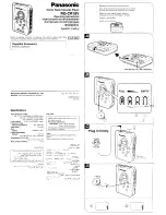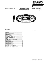
Service Manual
FILE NO.
REFERENCE No.
SM
5810290
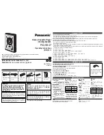
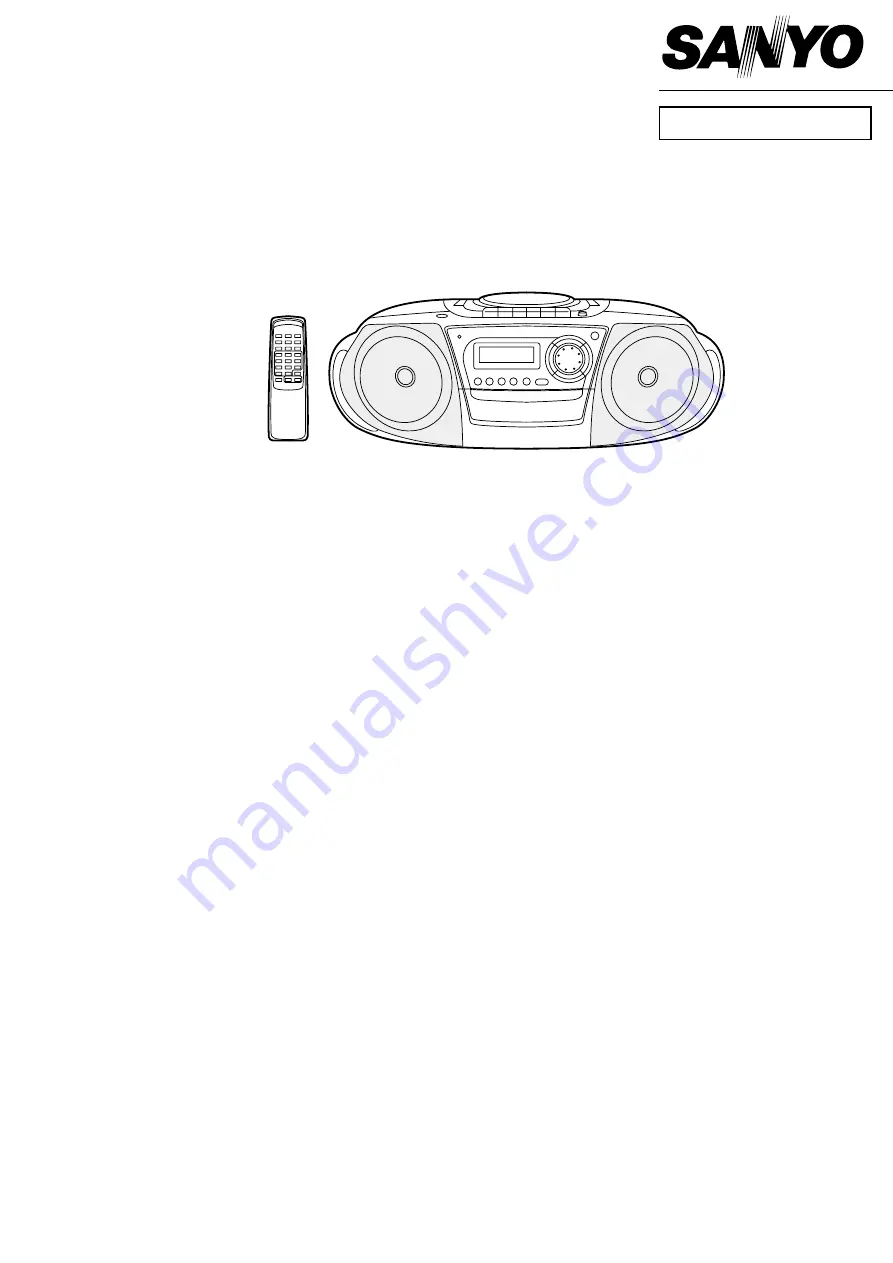
CD Portable Radio
Cassette Recorder
MCD-ZX700F
(XE)
PRODUCT CODE No.
164 081 00
CONTENTS
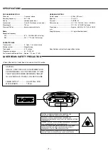
Specification ..................................................................... 1
Laser beam safety precaution .......................................... 1
Tuner Adjustment ............................................................. 2
Tape Deck Adjustment ..................................................... 3
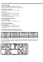
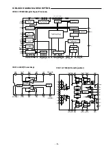
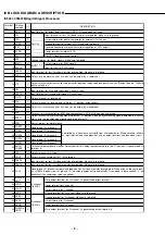
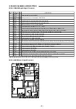
IC Block Diagram & Description ....................................... 3,7
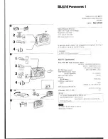
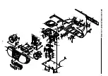
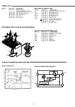
Exploded View (Cabinet & Chassis) ................................ 4
Parts List .......................................................................... 5
Exploded View & Parts List(Tape Deck) ......................... 7
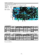
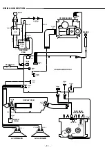
Wiring Connection ............................................................ 11
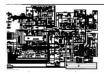
Schematic Diagram (Micom) ............................................ 12
Schematic Diagram (CD) ................................................. 14
Schematic Diagram (Radio) ............................................. 16
Schematic Diagram (Audio) ............................................. 18
Wiring Diagram (CD Main/Amp/Tu) ............................... 20
Wiring Diagram (Rectifier, Display, Power) .................... 21
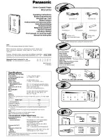
Summary of Contents for 164 081 00
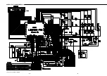
Page 13: ... 13 12 SCHEMATIC DIAGRAM DISPLAY This is a basic schematic diagram ...
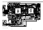
Page 14: ... 15 14 SCHEMATIC DIAGRAM CD This is a basic schematic diagram ...
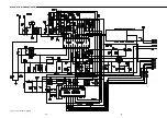
Page 15: ... 17 16 SCHEMATIC DIAGRAM TUNER This is a basic schematic diagram ...
Page 17: ... 20 WIRING DIAGRAM CD MAIN AMP TU CD MAIN AMP TU ...