background image

FILE NO.

Service Manual

CONTENTS

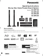
DVD Home Theater System

DC-TS960WL
DCS-HT900WL

(XE)

PRODUCT CODE No.
129 672 03 DC-TS960WL
129 672 04 DCS-HT900WL

REFERENCE No. 

SM

5810583

Laser beam safety precaution .......................................... 1

DVD Mechanism replacement ......................................... 2
Mechanism Replacement ................................................ 2

Wiring  Connection ........................................................... 5
Service mode ................................................................... 9

How to load software for system microcomputer ............. 13
How to load software for audio DSP ................................ 13

Tuner Adustment ............................................................. 14
Exploded View (Cabinet & Chassis : Main) ..................... 15

Parts List .......................................................................... 16
Exploded View (Cabinet & Chassis : Speaker Center) .... 20

Parts List .......................................................................... 20

Exploded View (Cabinet & Chassis : Speaker Front) ...... 21
Parts List .......................................................................... 22

Exploded View (Cabinet & Chassis : Speaker Rear) ....... 24
Parts List .......................................................................... 25

Exploded View (DVD Mechanism) ................................... 27
Parts List .......................................................................... 27

IC Block Diagram & Description ....................................... 28
Block diagram .................................................................. 48

Schematic Diagram .......................................................... 52
Wiring  Diagram ............................................................... 72

All manuals and user guides at all-guides.com

all-guides.com

Summary of Contents for 129 672 03

Page 1: ...em microcomputer 13 How to load software for audio DSP 13 Tuner Adustment 14 Exploded View Cabinet Chassis Main 15 Parts List 16 Exploded View Cabinet Chassis Speaker Center 20 Parts List 20 Exploded View Cabinet Chassis Speaker Front 21 Parts List 22 Exploded View Cabinet Chassis Speaker Rear 24 Parts List 25 Exploded View DVD Mechanism 27 Parts List 27 IC Block Diagram Description 28 Block diagr...

Page 2: ...KS DEFEATED AVOID EXPOSURE TO BEAM ADVARSEL USYNLIG LASER STRÅLING VED ÅBNING NÅR SIKKERHEDSAFBRYDERE ER UDE AF FUNKTION UNDGÅ UDS ÆTTELSE FOR STRÅLING VARNING OSYNLIG LASER STRÅLNING NÄR DENNA DEL ÄR ÖPPNAD OCH SPÄRR ÄR URKOPPLAD STRÅLEN ÄR FARLIG VORSICHT UNSICHTBARE LASERSTRAHLUNG TRITT AUS WENN DECKEL GEÖFFNET UND WENN SICHERHEITSVERRIEGELUNG ÜBERBRÜCKT IST NICHT DEM STRAHL AUSSETZEN VARO AVAT...

Page 3: ...ation DVD MECHANISM REPLACEMENT Connectors Do not connect or disconnect while power is on Connecting or disconnecting signal wires or the main power cord when the power is on may destruct the unit or fixture When connecting push all the way in securely An insufficient insertion may cause a bad contact leading to an erroneous operation Do not connect or disconnect roughly by an excessively strong f...

Page 4: ...the 2 tray Move the 1 slide to the left end Insert the 2 tray 4 4 3 5 1 2 ROUND HOLE MOTOR PULLEY SHASSIS HOLE TRIANGLE MARK SOLDERING MECHA P W B 1 Adjust the motor terminal to boss in the chassis 3 Adjust the round hole of the motor to the triangle mark of P W B and solder it CN002 SLED2 SLED1 GND LMT SW SP1 SP1 RED BLACK WHITE ORANGE BLACK RED 4 How to install the IF PWB All manuals and user gu...

Page 5: ...SF 106B GREASE CDF 409Z or SF 106B GREASE CDF 409Z or SF 106B Clean the groove by alcohol well A A A G SANKOL G SANKOL G SANKOL G SANKOL GREASE EM 30LG GREASE EM 30LG 6 Base mechanism mounting parts 7 Base mechanism parts 8 Tray parts MECHANISM REPLACEMENT All manuals and user guides at all guides com ...

Page 6: ... CONPONENT VIDEO OUT CN453 MONITOR OUT CN452 D1 D2 OUT CN454 CN603 9P CN406 3P CN611 3P CN607 6P CN606 9P CN601 10P CN498 2P CN495 9P CN497 2P CN496 PHONES CN241 10P CN201 CN203 2P CN900 7P CN100 24P CN162 6P MAIN P W B TUNER P W B WR950 BK WR951 WH CN951 2P FU950 P T POWER P W B FU401 2A 250V FU402 2A 250V AC IN AM LOOP ANT FM ANT CN455 14P SCART P W B UK XE Only CN661 A V EURO TV AUDIO IN CN660 ...

Page 7: ...CN401 CN406 4P CN400 9P CN252 9P CN251 8P CN253 5P CN291 5P CN405 8P CN501 8P CN500 CN404 2P CN300 2P F4600 125V 4A T2A L250V WIRELESS P W B ANT2 P W B SWITCH P W B MAIN P W B LED P W B SOCKET P W B CN407 2P This is a basic wiring connection All manuals and user guides at all guides com ...

Page 8: ... CN295 3P CN263 3P CN402 F4600 T1A L250V CN403 CN404 2P SPEAKERS IN R CH L CH REAR IN WIRELESS RECEIVER P W B ANT2 P W B AMP P W B ANT3 P W B AC IN POWER SWITCH ANT3 ANT2 LED P W B CN405 2P CN406 2P This is a basic wiring connection All manuals and user guides at all guides com ...

Page 9: ...ear Center SPEAKER TERMINAL CN601 4P CN602 2P CN300 2P SPEAKERS LED IN CN600 TERMINAL P W B LED P W B CN601 2P SPEAKERS IN CN600 SOCKET P W B Cnter Front Rear This is a basic wiring connection All manuals and user guides at all guides com ...

Page 10: ...d push FUNCTION button within 1 second A Market Region SETUP In the initial condition of this model Market information and other parameters such as Region code Tuner selection and RDS availability are undefined In the following cases Market information setup is necessary 1 When updating the system software using CD R Part code 0PRADC9671 2A 2 When replacing a main board While Market information is...

Page 11: ...n the right side of the Market denotation push numeric keys or cursor right and left keys on the remote controller to select Market code as listed on Market information setup table If you enter the wrong number just keep on inputting the numeric keys the inputted number displayed on the screen is shifted to the left Market code of this model is 02 3 2 Once the desired code is displayed push cursor...

Page 12: ...tion push cursor right or left key on the remote controller Information area updates in the following order JP2 US EU2 SS JP NX JP TV NX EU SS JP2 JP2 Notice This instruction should be proceed only if it is necessary Tuner selection of this model is EU2 6 Setting RDS Availability 6 1While a highlighted indicator is displayed on the right side of the RDS Availability denotation push cursor right or...

Page 13: ...y 8 1 Service mode entry mode displays Market information and software information on the screen Region 0 Region undefined or Region Free 1 6 Region Market JP WL depends on the selection Tuner JP2 depends on the selection RDS None depends on the selection VersionS30822A2 Brand S SANYO Version 30822 2003 8 22 Region 0 Region undefined or Region Free 1 6 Region SYSCON version Engineering department ...

Page 14: ...AUTION After replacing the Main P w Board ASSY Parts code 614 330 6658 should update both SYSTEM microcomputer software and AUDIO DSP software using latest update CD R respectively After replacing IC ASSY Parts code 410 521 4201 should update SYSTEM microcomputer software using latest CD R for SYSTEM microcomputer After replacing IC ASSY Parts code 410 495 7307 should update AUDIO DSP software usi...

Page 15: ... R2701 C2502 R2504 C2512 C2513 C2515 R2712 C2703 R2705 R2310 C2522 R2812 R2704 C2702 R2804 C2802 R2702 R2802 C2504 C2506 C2521 R2503 R2519 R2805 R2803 R2703 IC252 Q2502 C2803 XF23 3 XF231 TP24 TP25 TP12 TP11 L2151 a AM IN FM IN TP15 TP14 TP13 TP26 DC cut TUNER ADJUSTMENT 1 FM Standerd condition ANTENA 75Ω Unbalanced direct Mod Freq 1kHz Deviation MONO 22 5kHz STEREO 22 5kHz MAIN 6 75kHz PILOT RF L...

Page 16: ...14 51 53 54 55 60 56 57 58 59 Y01 Y01 Y01 Y05 Y05 Y05 Y02 Y05 Y06 Y06 Y06 Y06 Y07 Y07 Y08 Y09 Y09 Y10 Y11 Y12 Y13 Y13 Y13 Y15 Y15 Y14 71 73 72 74 75 76 77 55A 16 15 61 78 This is a basic exploded view All manuals and user guides at all guides com a l l g u i d e s c o m ...

Page 17: ...GHT 614 329 1718 CUSHION PAD SPACE TOP 614 328 3140 CUSHION SP CENTER FOR CABLE 614 328 3126 CUSHION TOP LEFT 614 328 3133 CUSHION TOP RIGHT 614 330 4999 INSTRUCTION MANUAL INST 900 614 330 4982 INSTRUCTION MANUAL INST 960 614 331 0785 INSTRUCTION MANUAL INST GREEK 900 614 331 0778 INSTRUCTION MANUAL INST GREEK 960 614 330 4951 CARTON CASE SX SX F R CENTER 900 614 330 4937 CARTON CASE SX SX F R CE...

Page 18: ...8 ASSY WIRE CN603 645 005 8141 PLUG 9P CN604 645 005 7373 PLUG 3P CN606 614 326 0301 ASSY WIRE CN607 614 328 4093 ASSY WIRE D6002 407 003 4507 DIODE DAP202K D6040 407 003 3609 DIODE DAN202K D6041 407 003 3609 DIODE DAN202K D6042 407 003 3609 DIODE DAN202K D6043 407 003 4507 DIODE DAP202K D6044 407 003 4507 DIODE DAP202K D6045 407 003 4507 DIODE DAP202K D6046 407 003 4507 DIODE DAP202K D6047 407 00...

Page 19: ...0B D4020 408 043 7902 DIODE G3SBA60L BU04 D4700 407 162 8507 DIODE DAN222 or 407 221 1906 DIODE KDS121E D4701 407 162 8507 DIODE DAN222 or 407 221 1906 DIODE KDS121E D4801 407 162 8507 DIODE DAN222 or 407 221 1906 DIODE KDS121E D4802 407 162 8507 DIODE DAN222 or 407 221 1906 DIODE KDS121E FPC41 645 031 7903 HOLDER FUSE or 645 006 4760 HOLDER FUSE FPC42 645 031 7903 HOLDER FUSE or 645 006 4760 HOLD...

Page 20: ...66 R NETWORK 10KX4 1 16W RN480 645 057 2166 R NETWORK 10KX4 1 16W RN481 645 057 2159 R NETWORK 1KX4 1 16W RN510 645 057 2166 R NETWORK 10KX4 1 16W RN511 645 057 2166 R NETWORK 10KX4 1 16W RN514 645 057 2166 R NETWORK 10KX4 1 16W RN515 645 057 2166 R NETWORK 10KX4 1 16W RN516 645 057 2159 R NETWORK 1KX4 1 16W RN801 645 057 2142 R NETWORK 100X4 1 16W RN802 645 057 2142 R NETWORK 100X4 1 16W RN803 64...

Page 21: ...CR S TPG BIN 3X10 SP UNIT Y03 411 021 3503 SCR S TPG BIN 3X10 COVER TOP TOP ELECTRICAL PARTS REF NO PART NO DESCRIPTION 51 645 062 5336 SPEAKER 4 8CM 52 645 062 5350 SPEAKER 8 TWEETER 53 614 327 8726 ASSY WIRE 8CM SERIES CONNECT 54 614 327 8719 ASSY WIRE 8CM TO TERMINAL 55 645 062 5534 TERMINAL 2P 614 327 8245 ABSORPTION Y04 411 098 4700 SCR S TPG BIN 2 3X8 STAND CENTER Y06 411 021 3701 SCR S TPG ...

Page 22: ... Y16 Y16 Y16 Y17 Y20 Y19 Y19 Y18 Y18 Y18 Y18 Y18 Y18 Y17 18 9 19 20 74 75 77 21 22 23 6 4 8 10 11 Y10 12 14 14 14 14 14 14 58 59 60 61 1 2 Y01 Y04 Y06 Y08 Y08 Y08 Y08 Y09 5 53 62 54 55 56 57 62 7 15 16 17 Y11 Y13 Y12 Y15 Y16 Y16 Y16 Y20 Y19 Y19 18 9 19 20 74 76 21A 23 6 8A 11 Y10 14 14 14 14 14 14 58 11 Y10 11 Y10 15A 15A 71 All manuals and user guides at all guides com ...

Page 23: ...O DESCRIPTION 72 614 327 7590 ASSY PWB SWITCH Only initial CN291 645 005 9292 PLUG 5P S2901 645 062 2700 SWITCH ROTARY LED P W BOARD ASSY REF NO PART NO DESCRIPTION 74 614 327 8405 ASSY PWB LED Only initial CN300 645 006 0908 PLUG 2P D3000 408 044 9100 LED HLMP EL31 SVK00 SOCKET P W BOARD ASSY REF NO PART NO DESCRIPTION 75 614 327 8412 ASSY PWB SOCKET Only initial CN500 645 064 1183 SOCKET MIN 8P ...

Page 24: ...2515 PROTECTOR 0 2A 125V PR461 645 042 2737 PROTECTOR 7A 125V PR462 645 042 2515 PROTECTOR 0 2A 125V PT400 645 061 9335 TRANS POWER PULSE Q4601 405 159 0503 TR KRC107S or 405 141 5608 TR DTC114YKA Q4602 405 151 6107 TR KRA107S or 405 141 5707 TR DTA114YKA Q4603 405 141 3604 TR KTA1273 Y or 405 009 5207 TR 2SB927 S or 405 009 5306 TR 2SB927 T Q4900 405 146 2107 TR KTC3875 Y or 405 146 2206 TR KTC38...

Page 25: ...12 12A 13 13 71 72 71 74 75 51 52 53 53 54 54 55 55 55 55 56 56 57 58 14 59 Y01 Y01 Y02 Y03 Y04 Y06 Y06 Y07 Y07 Y07 Y07 Y08 Y08 Y08 Y08 Y08 Y08 Y09 Y09 Y09 Y09 Y10 Y10 Y11 Y11 Y12 Y12 Y13 Y14 Y14 Y16 Y16 Y16 Y16 Y17 Y17 Y14 Y05 Y05 Y15 Y15 Y15 Y15 Y15 Y15 All manuals and user guides at all guides com ...

Page 26: ...6 1407 TR KRC104S or 405 138 6700 TR DTC144EKA Q2952 405 146 1407 TR KRC104S or 405 138 6700 TR DTC144EKA MAIN P W BOARD ASSY REF NO PART NO DESCRIPTION 74 614 330 4647 ASSY PWB MAIN Only initial C4000 403 349 3303 CERAMIC 0 01U M 250V or 403 366 7803 CERAMIC 0 01U M 250V C4005 403 325 0302 ELECT 2200U M 25V C4600 404 088 7607 MT POLYEST 0 22U K 250V C4601 404 080 8107 CERAMIC 2200P M 400V C4603 4...

Page 27: ...06 TR KTC3875 GR or 405 014 4509 TR 2SC2412K R or 405 011 1006 TR 2SC1623 L6 Q4901 405 146 2107 TR KTC3875 Y or 405 146 2206 TR KTC3875 GR or 405 014 4509 TR 2SC2412K R or 405 011 1006 TR 2SC1623 L6 Q4902 405 146 2107 TR KTC3875 Y or 405 146 2206 TR KTC3875 GR or 405 014 4509 TR 2SC2412K R or 405 011 1006 TR 2SC1623 L6 Q4905 405 151 6107 TR KRA107S or 405 141 5707 TR DTA114YKA Q4906 405 159 0503 T...

Page 28: ...1607 SCR S TPG PAN PCS 1 7X4 DM21 614 310 2083 GEAR RACK MOVE PICKUP FREE DM22 614 310 6159 SPRING COMP FOR BACK RUSH RACK DM23 614 310 2076 GEAR RACK MOVE PICKUP FIX DM24 411 018 4704 SCR PAN PCS 1 7X5 LIMIT SW FIX DM25 645 040 9899 SWITCH MICRO 1P 2T LIMIT SW DM26 412 057 8304 SPECIAL WASHER FOR GEAR 2 FIX DM27 614 310 2069 GEAR GEAR 5 DM28 614 310 6142 SPRING COMP FOR BACK RUSH DM29 614 310 205...

Page 29: ...k b f m g c e r p n d Dp col 10G a h j k b f m g c e r p n d Dp col 11G ANODE CONNECTION PIN CONNECTION 54 NX NX NX NX NX NX NX NX NX NX NX NX 11G10G 9G 8G 7G 6G 5G 4G 3G 2G 1G NP NP NX F1 PIN NO CONNECTION PIN NO CONNECTION 27 26 25 24 23 22 21 20 19 18 17 16 15 14 13 12 11 10 9 8 7 6 5 4 3 2 1 F2 NX NP NP P1 P2 P3 P4 P5 P6 P7 P8 P9 P10 P11P12P13 P14P15P16 P17 NX NX NX NX NX NX 54 53 52 51 50 49 ...

Page 30: ... VCC VCC GU AG0F AG0F PREF FC BST DVD CD 1K 1K 47K 47K 47K 47K 6P 6P 47K 47K 680 680 LDON2 LDON1 CDTH TEBL TEBL LDTH LDON1 LDON2 AGOF BCA GU DVD CD DPD TE WO PP VCC TH XHTR SGC TEBL FEBL FC BST SREFI SREF 270P 4 3K SREF FEBL 1K 1K FEBL PREF PREF SREF SREF 23K 23K 87P 87P 1K 1K SREF 76K 76K 10P 10P SGC GU SGC GU SGC GU SGC GU SREF SREF TH BCA 280K 58K 30KHZ 200KHZ 30KHZ 200KHZ DPD TE XHTR XHTR SREF...

Page 31: ...output Push pull output Push pull gain setting resistor connect DC cut capacity connect BPF center frequency setting resistor connect RF bottom detection output RF peak detection output SREF setting Peak hold detection setting resistor connect When SCA RF AGC PH detection conderser connect Servo signal voltage reference output RE DC servo condenser connect N C RF output RF output Ground RF system ...

Page 32: ...DCKIO VPDO VCOC VRFFR HDAT 7 0 HADR 12 0 HRDB HWRB HCSB HWAITB HIRQOB FDO TDO SLDO SPDO SGC TBAL FBAL BST FO TSTDO TSTDI TESIO HFLIO EMPH FSX EFLG DOUT LRSY ROMCK ROMXA C2F MRASIB MCASUB MCASLB MOEB MWEB MD 15 0 MA 12 0 AVACKO AVREQI AVDACK AVSCTB AVERRB AVD 7 0 A D Block D A Block Servo Block SLC Block 8 bits A D 8 bits D A Servo DSP 16x16 32 32 MPX RF I F Block FC Counter TR Counter EV Counter F...

Page 33: ...requency comparison filter connect Filter connect 1 Filter connect 2 Filter connect 3 Voltaji moniter Charge pump PCH control voltage Constant current charge pump current set of phase comparison Constant current charge pump current set of frequency comparison EFM playback PLL VCO oscillation renge set CD EFM playback PLL VCO oscillation range set DVD EFM PLL JV power supply Analog 3 3V Analog GND ...

Page 34: ... VCC VEE IN A IN A OUT A A B IC420 424 NJM2058 Operation Amp 1 2 3 4 11 12 13 14 A OUTPUT A INPUT V C INPUT A INPUT B INPUT D INPUT V D INPUT D OUTPUT A D 5 6 7 8 9 10 B INPUT B OUTPUT C INPUT C OUTPUT B C IC241 LC7212M D PLL 2 1 24 17 16 3 4 5 6 18 15 7 8 9 10 11 14 19 20 21 22 13 Vssx XIN XOUT FMIN AMIN CE DI CL DO VDD Vssd PD AIN AOUT Vssa IFIN IO1 IO2 BO1BO2 BO3 BO4 PHASE DETECTOR CHARGE PUMP ...

Page 35: ... 27 OE Input Output Enable 2 5 7 10 31 34 36 39 I O0 I O15 Input Output Data Input Output 1 6 20 VCC Supply Power 3 3V 21 35 40 VSS Ground Ground 11 12 15 30 NC No Connect CONTROL LOGIC DATA IN BUFFER CLOCK GENERATOR DATA OUT BUFFER COLUMN ADDRESS BUFFER REFRESH CONTROLER REFRESH COUNTER ROW ADDRESS BUFFERS 9 9 A0 A1 A2 A3 A4 A5 A6 A7 COLUMN DECODER OE 16 ROW DECODER 512 x512 x 16 MEMORY ARRAY 16 ...

Page 36: ... VIN1 No 19 20 21 22 23 24 25 26 27 28 29 30 31 32 33 34 35 36 Function CH2 InputĂInput OP AMP Input CH2 InputĂInput OP AMP Input CH2 InputĂInput OP AMP Output CH3 InputĂInput OP AMP Input CH3 InputĂInput OP AMP Output OP AMPĂOutput OP AMPĂ Input OP AMPĂ Input Regulator Error AMP Output Fxternal PNP transistor base Regulator Error AMP Input VREF_AMP Voltage follow up Output VREF InputĂExternal PNP...

Page 37: ... 2 Anode 3 Cathode 2 3 IC404 405 KIA7805 7809 5V Regulator 1 INPUT 2 COMMON 3 OUTPUT 1 2 3 IC602 M34506M2 728FP Micon 1 2 3 4 5 6 7 8 9 10 20 19 18 17 16 15 14 13 12 11 P00 I O P01 I O P02 I O P03 I O P10 I O P11 I O P12 CNTR Timer output P13 INT Interrupt input D0 I O D1 I O VDD VSS GND XIN Clock input XOUT Clock output CNVSS GND RESET P21 AIN1 I O P20 AIN0 I O D3 K I O D2 C I O All manuals and u...

Page 38: ... Tripath recommends using a value of 100 F for the bulk capacitor VN10 generator filter inductor This inductor sized appropriately so that LSW does not saturate If the recommended inductor value of 100 H is not used the VN10 may overshoot with respect to VNN during TA2022 turn on Flywheel diode for the internal VN10 buck converter This diode also prevents VN10SW from going more than one diode drop...

Page 39: ...SP input terminal 2ch DSP MIX input terminal DSP surround Rch input terminal DSP surround Lch input terminal DVD center speaker input terminal DSP sub woofer input terminal Analog ground terminal Sub woofer input gain output terminal Sub woofer volume input terminal Analog ground terminal Center speaker input gain output terminal Center sspeaker volume input terminal Sub woofer output terminal Cen...

Page 40: ...p LPF 2Step Amp 2 LPF1 2Step Amp 3 2Step Amp 5 2Step Amp 4 LPF1 LPF2 LPF1 LPF2 LPF1 MIX DRIVER DRIVER DRIVER DRIVER DRIVER DRIVER PEDESTAL CLAMP PEDESTAL CLAMP 2Step Amp 6 LPF2 LPF1 PEDESTAL CLAMP REG VCC SYNC SEP IC481 MM1508XNRE Switing 6 IN1 4 IN2 1 5 GND SW 3 Vcc 2 OUT Clamp Clamp Bias DRV 6dB IC495 NJM4556AL Op Amp 1 2 3 4 8 7 6 5 A B D M V Type Top View V V IC490 811 603 PST3627U Op Amp OUT ...

Page 41: ... Byte Enable Input DQ9 to DQ16 Output Enable Input Power Ground No Connection Pin No 1 5 18 22 24 27 4 2 44 6 7 10 13 16 29 32 35 38 17 39 40 41 11 33 12 34 23 28 Pin Descriptions CE OE HB LB WE Symbol A0 A16 CE DQ1 DQ16 WE LB HB OE VCC GND NC Decoder 512 x 4096 Memory Array Input Data Circuit Column I O Input Data Circuit Control Circuit 3 1 2 Control part GND DC INPUT Vin DC OUTPUT Vo IC900 PQ03...

Page 42: ...ly Filter Capacitor Connection Recommended 10 F 100nF Reference Filter Capacitor Connection Recommended 10 F 100nF ADC Left Channel Negative Input ADC Left Channel Positive Input ADC Right Channel Negative Input ADC Right Channel Positive Input ADC Master Slave Positive Input Auxiliary DAC Output Data DAC LR Clock DAC Bit Clock Digital Ground DACx Input Data Left and Right Channels Auxiliary ADC3 ...

Page 43: ...in When L the AK4112B is powered down and reset External Resistor Pin 18 1 resistor to AVSS externally Analog Power Supply Pin Analog Ground Pin Receiver Channel 1 This channel is selected in Parallel Mode or default of Serial Mode Audio Data Interface Format 0 Pin in Parallel Mode Receiver Channel 2 in Serial Mode Audio Data Interface Format 1 Pin in Parallel Mode Receiver Channel 3 in Secial Mod...

Page 44: ...s pin outputs scrial data at the falling cdge of the shift clock starting from the lower bit Data Input Pin This pin inputs serial data at the rising cdge of the shift clock starting from the lower bit Clock Input Pin This pin reads serial data at the rising cdge and outputs data at the falling cdge Serial Interface Strobe Pin The data input after the STB has fallen is processed as a command When ...

Page 45: ...uts Outputs No Connect Pin Names OEn LEn I0 I15 O0 O15 NC IC812 AT24C08N 10SJ 2 7 2 Wire Srial 8 VCC 4 GND 7 WP 3 A2 2 A1 1 A0 6 SCL 5 SDA DEVICE ADDRESS COMPARATOR START STOP LOGIC SERIAL CONTROL LOGIC H V PUMP TIMING DATA RECOVERY EEPROM SERIAL MUX DOUT ACK LOGIC Y DEC Function Address Inputs Serial Data Serial Clock Input Write Protect No connect Pin Name A0 A2 SDA SCL WP NC DATA WORD ADDR COUN...

Page 46: ...V Ground Pin A0 A18 Q0 Q14 Q15 A 1 CE WE BYTE RESET OE RY BY VCC GND ADDRESS LATCH AND BUFFER SENSE AMPLIFIER PGM DATA HV PROGRAM DATA LATCH I O BUFFER Y PASS GATE ARRAY SOURCE HA MX29LV800T B MX29LV800AT AB FLASH ARRAY X DECODER X DECODER COMMAND DATA DECODER COMMAND DATA LATCH STATE REGISTER WRITE STATE MACHINE WSM PROGRAM ERASE HIGH VOLTAGE CONTROL INPUT LOGIC 28 OE 11 WE 12 26 CE RESET 1 8 16 ...

Page 47: ...ring row address latch time Select bank for read write during column address latch time Latches row addresses on the positive going edge of the CLK with RAS low Enables row access precharge Latches column addresses on the positive going edge of the CLK with CAS low Enables column access Enables write operation and row precharge Latches data in starting from CAS WE active Makes data output Hi Z tSH...

Page 48: ...X SO OE VDD Description GND N C Serial Data Shift clock for shift register Trailing edge trigger Latch clock for storage register Trailing edge trigger Parallrl data output Nch Openn Drain FET Serial data output Output enable control input Power spply I O I I I O O I Latch Output FET L ON H OFF Notes OE Pull down to VSS Control circuit Output buffer Open drain 12 bit Storage register 12 bit Shift ...

Page 49: ... 2 SPDIF CD DREQ KFG AD0 FDO TDO SLDO SPDO RDY INT_DEC WRQ LSI_RST HD 0 15 HD 0 15 HA 0 15 HA 16 19 RD WR RD WR BSEL0 CE 1LE 2LE 1LE 2LE 3 3V CS_DVD CS_DVD FSEL AMCLK 16 9344M 27M ACLKI 512FS 3 3V 3 3V SPDIF29 SPDIF30 DIR_DO MCLK LRCK DIR_BCLK DSP_CLK DSP_DOUT DSP_DIN DIR_CE DIR_RST DIR_CE DIR_RST DSP_CE LSI_RST DSP_CE LSI_RST DSP_IRQ CODEC_CE CODEC_RST CODEC_CE CODEC_RST DSP_CLK DSP_DOUT DSP_DIN ...

Page 50: ...A2022 KIA4558 KA431A KIA7805 STR F6238S TA2022 PST3627 PST3645 WIRELESS MODULE TX TX ANT WIRELESS MODULE RX RX ANT DRAIN VIN F B GND VPP 12V 9V 5V VNN 12V C SL SR FR FL SO_SW GND DC_IN SW SP RY 12V WIRE AGND P RY 12V VPP VPP VNN VNN VPP VPP 12V 12V FL FR C SW DC_IN SP_RY SP_RY PCON NC LCH DET1 DET2 AGND RCH SL SR DET WIRE SP_RY PCON RCH AGND LCH DET1 DET2 NC PCON SP_RY SP_RY PCON SL SR 9V 9V DET W...

Page 51: ... 0 1 75 470 0 1 47 6 3 82K 82K 1 8 2K 1K 10K 220P 220P 1 8 2K 1K 10K NJM4558 NJM2058V 1K 4 7K 1 100K 0 022 18K 4 7K 100P 0 1 10K 1K 4 7K 12K 4 7K 4 7K 56P 12K 12K 56P 1K 10K 0 1 100P 100P 0 1 10K 1K 100K 100K 100K 100K 47 25 47 25 100K 100K 100K 100K 10 25 NJM4558 39K 47P 9 1K 100P 100P 39K 47P 100K 100K 9 1K 10 25 100K 10 25 47P 39K 9 1K 100P 100K 36K 0 01 100K 0 022 1 2K NJM2058V 47 25 47 25 9 1...

Page 52: ...K 0 100 100 100 10 10K 10K 10K 33 0 1 1000 10K 47 6 3 0 1 0 0 1 MX29LV800ATTC 70G 0 0 10K 10K 10K 1K 0 1 1000 150 6 3 0 1 0 1 33 104 ADSST MEL322 40 Melody 32 1 2 3 4 5 6 7 8 9 10 11 12 13 14 15 16 17 18 19 20 21 24 48 47 46 45 44 43 42 41 40 39 38 37 36 35 34 33 32 31 30 29 28 25 5 28 29 30 31 32 33 34 35 36 37 38 39 40 41 42 43 44 45 46 47 48 21 20 19 18 17 16 15 14 13 12 11 10 9 8 7 6 5 4 3 2 1...

Page 53: ...100 100 100 100 100 10K 10K 10K 33 33 33 47 10K 1K 0 1 100 100 100 100P 100P 100P 100P 0 01 0 01 0 01 0 01 0 01 0 01 0 01 0 01 19 20 21 24 30 29 28 25 5 28 29 30 21 20 19 1 2 3 4 8 7 6 5 156 155 154 153 152 151 150 149 148 147 146 145 144 143 142 141 140 139 138 137 136 135 134 133 132 131 208 207 206 205 204 203 202 201 200 199 198 197 196 195 194 193 192 191 190 189 188 187 186 185 184 183 182 1...

Page 54: ... C4524 CN422 R4836 D4802 0 1 0 1 0 1 10K 0 0 470 470 470 470 470 470 100P 100P 100P 0 022 100P 100P 100K 100P 9 1K 47P 100K 100K 39K 47P MM1508 470 6 3 0 1 0 1 220 220 220 75 75 1K 220 6 3 0 01 0 1 10K 100 1000 0 01 6 3 0 1 0 1 LA73054 E 0 01 0 1 1K 1K 100K 100K 10 22K 100P 100P 22K 39K 22K 100P 100P 39K 22K 1608SGX 1608SGX 75 75 47 6 3 47 6 3 39K 39K 1608SGX 1608SGX 1608SGX 1608SGX SGX 08SG 75 75...

Page 55: ...0 047 0 047 0 047 0 047 150 150 PQ12DZ5U 06 07 10u 0 1 0 1 0 1 0 1 0 1 150 6 3 0 1 K4S6641632F TC75 000 0 1 BU2099FV 10K 14 0 0 100 1000 0 01 6 3 0 1 160 SGX 1608SG 75 GP1FP313RK 1000 0 1 75 470 0 1 47 6 3 0 01 1000 1000 6 3 1000 KRC107S 11 14 3 2 1 1 2 3 1 2 3 4 5 5 4 3 2 1 1 2 3 4 5 1 2 3 4 5 1 2 3 4 5 6 1 2 3 4 5 6 7 27 26 25 24 23 22 21 20 19 18 17 16 15 14 13 12 11 10 9 8 7 6 5 4 3 2 1 54 53 ...

Page 56: ...00P 100P 100P PT6315 SURRUND STOP INPUT 0 01 SPS 440L 1 HG 47 10 16 0 01 10 10 2 2K 4 7K 220P P_CHK 1AV4T41B06700 DAN202K DAN202K DAN202K DAP202K DAP202K 82K 100K 100K 100K 10K 10K CTRL ST KEY MUTE CTRL2 CTRL1 CTRL0 0 01 0 1 PST3627UR 100P 4 7K 09 TRAY PLAY 100P 100K KRA107S DAP202K KRA107S DAP202K KRA107S KRA107S DAP202K KRA107S KRA107S KRA107S DAP202K DAP202K 0 1 1 8K 1 2K 47 50 47 50 03 06 09 2...

Page 57: ...0 01 1 5K KTC3193 1 8K 0 01 560 0 01 1K 10K 3 3K 100 100 1000P 1000P 220 6 3 220 6 3 NJM4556AL 100K 100K 47K 3 3K 3 3K 47K KTD1303 KTD1303 100 100 22P 22P 100P 10U 10U 22U 0 1 0 1 1608SGX 9 02 KTD1303 100 120 KTD1303 120 100 1000P 1000P 0 01 100 1K 47K 3 3K MTZJ13B KTC3227 07 KRA107S 47K 33K 0 047 2 2 50 2 2 50 1 2K KTA1274 MTZJ30B 220 63 220K MPG06G DF06S 0 1 0 1 1AV4F35B0950N 2 2K KTC3875 82K 1 ...

Page 58: ...3 R1012 R1835 R1834 C1821 R1833 R1832 C1820 R1009 R1008 R1017 R1830 R1831 CAP R1073 C1047 R1075 R1018 R1019 R1016 C1042 C1043 C1822 C1048 R1072 R1076 C1046 R1074 C1000 C1001 C1002 C1003 R1800 R1801 C1004 R1014 R1015 R1704 R1700 R1701 R1703 R1705 D1700 C1701 C1550 C1012 BH ADBH WO ADTE TEC SGC TOST FOST HFLIO TESIO LDON2 LDON1 XHTR WRQ DEFECTO DVD_ CD C1845 C1846 C1847 INT_DEC RDY LSI_RST RD WR CS_...

Page 59: ...70 EGP10D 0 1 B EGP10D EGP10D 0 1 B EGP10D 270 47 16 0 47 J G 6 2 0 22 J G 10 M 0 1 B 0 1 B 8 2K 200K 1 16F 200K 1 16F 47 16 22K 18K 1 50 0 1 B 22K 18K 4 7 50 1 2K 1 2K 330P CH 1K 1K 6 98K 1 16F 6 98K 1 16F 120P CH 1 2K 1 2K 6 98K 1 16F 6 98K 1 16F 1K 1K 10K 10K 47K 47K TA2022 0 1 B EGP10D 0 1 B 100 35 0 1 100B 0 1 100B 0 1 B 1000 50 0 1 B 1000 50 10 M EGP10D EGP10D 0 22 J G 6 2 0 47 J G 270 EGP10...

Page 60: ...22 0 1 B EGP10D 0 1 B 100 35 0 1 100B 0 1 100B 0 1 B 1000 50 0 1 B 1000 50 10 M EGP10D EGP10D 0 22 J G 6 2 0 47 J G 270 EGP10D 0 1 B EGP10D EGP10D 0 1 B EGP10D 270 47 16 0 47 J G 6 2 0 22 J G 10 M 0 1 B 0 1 B 8 2K 200K 1 16F 200K 1 16F 47 16 22K 8 2K 4 7 50 0 1 B 22K 8 2K 4 7 50 1 2K 1 2K 330P CH 1K 1K 6 98K 1 16F 6 98K 1 16F 120P CH 1 2K 1 2K 6 98K 1 16F 6 98K 1 16F 1K 1K 1K 100 K G5SBA60 5D2 14 ...

Page 61: ...RN833 RN832 RN831 RN830 RN830 RN830 481 15 C4 481 15 C4 CN710 C C N N 7 7 1 1 0 0 CN710 RN710 RN710 RN71 866 R8 63 866 R8 63 866 R8 62 866 R8 62 866 64 R8 866 64 R8 803 8034 R8 803 8034 R8 802 22 C8 802 22 C8 IC851 C851 IC8 IIC C851 51 C851 860 01 R8 860 01 R8 850 0 2 R8 8 50 0 2 R8 IC841 IC I 480 0 2 R4 4 80 0 2 R4 RN481 480 0 4 R4 4 80 0 4 R4 RN480 481 1 0 R4 4 81 1 0 R4 480 0 6 C4 4 80 0 6 C4 C...

Page 62: ... 451 C4 445 451 R4 4 45 451 R4 440 0 1 C4 4 40 0 1 C4 440 0 1 R4 4 40 0 1 R4 421 4 11 C4 421 4 11 C4 426 6 61 C4 426 26 61 C4 431 1 11 C4 431 1 11 C4 436 4 61 C4 436 4 61 C4 446 4 61 C4 446 4 61 C4 441 1 11 C4 441 1 11 C4 454 41 R4 454 41 R4 454 4 3 R4 4 54 4 3 R4 424 4 40 R4 4 24 4240 R4 CAN03 CAN03 CA CAN0 AN0 N0 CA CAN04 C N04 CA CAN0 0 CAN0 CA Q4227 Q 7 Q Q Q 445 4450 R4 445 4450 R4 440 40 0 2...

Page 63: ...0 0 6 C4 IC471 71 4 1 1 C IC C C C 1 1 1 1 1 1 1 1 1 1 1 1 1 C C 7 IC472 2 2 2 IC IC 2 2 2 2 C C C 2 2 2 2 2 2 C C 72 425 253 R4 4 25 253 R4 420 20 4206 R4 4 20 20 4206 R4 430 30 4306 R4 4 30 30 4306 R4 430 303 R4 4 30 303 R4 425 4 56 R4 4 25 4256 R4 3 6 3 6 420 20 0 3 R4 4 20 20 0 3 R4 435 356 R4 4 35 356 R4 445 445 5 6 R4 4 45 445 5 6 R4 440 403 R4 4 40 403 R4 435 353 R4 4 35 353 R4 445 4 53 R4 ...

Page 64: ...21 R 102 2 6 C1 1 02 2 6 C1 106 6 0 R1 1 06 6 0 R1 82 82 82 2 4 R18 8 2 82 R1 24 182 106 67 R1 106 67 R1 102 1 29 C1 1 02 1029 C1 106 065 R1 1 06 065 R1 106 6 1066 R1 1 06 6 1066 R1 R1823 R 103 030 C1 103 030 C1 108 83 R1 108 83 R1 4 34 3 04 1 41 C1 1 04 1 41 C1 1 C1 1 C1 C10 101 012 C1 101 012 C1 R1810 1810 R R R 800 1800 R1 R1 R1 180 R180 01 R R R 188 888 R1 1 88 888 R1 1 R18 R 831 R R R183 R18 ...

Page 65: ... 10 0 10 03 1 0 10 03 85 50 01 R8 85 50 01 R8 850 0 6 C8 8 50 0 6 C8 850 8505 C8 8 50 8505 C8 850 02 C8 850 02 C8 850 8 04 C8 850 8 04 C8 850 07 C8 850 07 C8 850 0 3 R8 8 50 0 3 R8 804 C8 47 804 C8 47 804 C8 45 804 C8 45 804 C8 44 804 C8 44 80 0 4 C8 42 80 0 4 C8 42 803 8 C8 37 803 80 C8 37 803 03 C8 36 803 03 C8 36 804 04 C8 43 804 04 C8 43 804 C8 41 804 C8 41 802 02 R8 23 802 02 R8 23 802 22 R8 ...

Page 66: ... C4506 06 C45 5 06 C C 4506 06 C 506 C C C45 C4504 C45 C4504 C C 45 C4504 504 C C C4505 50 C C 45 C 505 C C 4505 50 C 505 C C C45 4 C 507 C45 45 5 07 C C 45 4 C 507 507 C C C8 8 308 C8 8 3 3 08 C C 8 8 308 308 C C C8 8 307 C83 83 3 07 C C 8 8 307 307 C C C83 3 3 0 C C 8305 C 305 C8305 C 30 305 C C C80 80 C 02 C C 8 8 024 4 C8 8 024 024 C C C48 8 0 C C 4801 1 C4801 801 C C C48 8 0 C C 4802 2 2 C480...

Page 67: ...031 R6031 DS601 CN604 JOG_A JOG_B GND 1 2 3 CN607 CN606 CN601 1 5 6 7 8 9 10 11 12 13 14 15 34 35 36 37 38 39 40 41 42 43 44 45 46 47 48 49 50 54 E E E C C C B B B B B C C E E E E C C B B B B C C E E E C B B C E E C B PLAY STOP F SKIP R SKIP SURROUND INPUT TRAY 1 2 IC602 R6054 R6053 C6052 R6002 C6066 R6006 R6007 R6004 R6005 R6003 R6001 C6004 C6002 C6032 R6032 R6055 R6056 IC603 C6064 C6065 R6057 Q6...

Page 68: ...J2214 J2009 J2204 J2422 J2205 J2408 J2404 J2401 J2202 J2405 J2403 J2423 J2428 J2201 C2305 C2321 IC231 XF231 R2302 R2309 C2302 J2003 XF222 C2303 XF233 Q2201 L2101 J2001 J2415 XF221 L2151 C2102 J2402 LC72121 0VADJ LA1844 J2002 J2417 J2213 J2425 J2421 J2407 J2411 J2400 J2418 R2114 C2317 C2311 C2307 J2000 J2424 J2004 J2203 J2406 CN203 J2416 J2019 J2018 R2202 D2151 C2465 C2451 C2301 J2208 J2212 J2020 J...

Page 69: ...4601 D4600 TH460 C4600 F4600 R4939 R4613 IC402 L4600 R4604 R4603 C4607 C4614 C4918 C4920 L4601 L4602 L4500 L4400 L4800 L4700 C4933 C4904 C4906 C4947 C4946 C4945 L4941 C4942 D4940 C4943 Q4941 Q4940 C4941 L4940 CN402 C4617 Q4946 CN405 L4603 R4619 C4603 C4604 PR462 R4618 PR461 C4404 C4504 C4804 C4704 C4626 D4608 CN400 CN407 CN406 CN404 L4946 L4943 L4948 L4945 HS402 HS403 WR 402 C4629 D4941 L4949 PC40...

Page 70: ...812 R4923 Q4901 Q4902 R4922 Q4900 CAN CAN CAN CAN CAN CAN Q4602 Q4601 R4800 R4700 R4506 R4504 R4502 R4915 R4913 R4918 R4917 R4912 R4914 C4923 R4916 C4925 C4926 R4503 R4501 R4505 C4502 R4402 R4406 R4404 R4405 R4403 R4401 C4402 C4922 R4500 C4500 C4917 C4919 C4921 C4914 R4400 C4400 IC400 R4955 R4954 R4953 R4951 R4952 C4944 R4950 R4944 R4945 R4943 R4941 R4942 R4947 R4946 R4948 R4949 C4940 R4940 C4625 ...

Page 71: ...622 D4609 R4614 Q4603 C4803 R4807 C4808 D4800 D4801 D4900 C4701 D4702 C4801 D4802 C4703 R4707 C4708 D4700 D4701 SVR48 SVR47 C4910 C4913 C4906 C4933 C4901 L4800 C4000 RY400 C4006 D4000 C4005 D4002 D4004 D4003 D4001 D4906 RY402 Q4601 PR402 D4611 R4616 C4625 C4904 L4601 L4602 L4700 C4928 C4612 L4900 D4005 D4006 CN404 L4603 L4600 C4600 C4631 R4619 C4704 PT400 CN403 HS401 HS402 C4805 C4806 C4706 C4705 ...

Page 72: ...003 C4001 R4936 R4935 C4626 CAN CAN CAN CAN CAN CAN Q4900 R4922 Q4902 Q4901 R4923 R4921 Q4005 R4939 R4940 R4941 C4934 Q4905 Q4906 R4938 Q4907 C4914 CAN C4605 C4627 R4942 C4807 C4707 CAN CAN R4820 R4818 R4819 R4719 R4720 CAN CAN R4718 Q4701 R4717 R4817 Q4801 R4943 Q4910 Q4908 R4944 R4945 Q4909 R4937 R4003 R4006 IC490 Q4911 Q4912 IC491 Q4004 C4982 C4983 C4981 C4980 C4972 CAN C4970 CAN C4966 C4964 R4...

Reviews: