ADJUSTMENT MANUAL
Specifications
Televialon ayatem
Video recording
ayatem
Audio recording
ayatem
CaHette type
Tape apeed
Maximum recording
time
Faat forward/
Rewind time
Image aenaor
Viewfinder
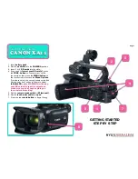
Lena
Filter diameter
Focua
White balance
lria
Minimum subject
illumination
PAL,
CC
I
R
Rotating 2-head, helical-scan
system
Rotating head,
FM
system
8 mm video cassette tape
S P : approx. 20.051 mm/sec.
L P: approx. 1 0.058 mm/sec.
90 minutes (P5-90 cassette) SP mode
180 minutes (P5-90 cassette) LP mode
Approx. 6.5 minutes
(PS-90 cassette)
. CCD
solid-state type (470,000 pixels)
0.6 inch electronic viewfinder
{black and white)
1 2X power zoom lens F 1 .8
(f= 5.0 to 60 mm)
49 mm
Fuzzy logic auto focus
Full auto fuzzy logic
Fuzzy logic auto iris
3 lux (Low light mode)
No.
\ 4- \re
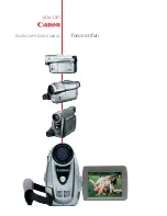
8 mm Camcorder
VM-EX70P
(EUROPE)
(AUSTRALIA)
(NEW ZEALAND)
Subject illumination
3 - 1 00,000 lux
range
Recommended
300 lux or more
aubject illumination
Power aupply
6 V : battery pack
6.5 V : AC adaptor/charger
Power conaumptlon
6.4
W
during camera recording
Operating
o
'C
- 40
'C
(32 'F - 1 04 ' F)
temperature range
Storage temperature
-20
'C
-
60
'C
range
( -4 'F - 1 40
'F)
Dimenaiona
{W)
x
(H)
x
(0)
Weight
Microphone
Video output
terminal
Audio output
terminal
S-Video output
terminal
121
x
1 1 1
x
208 mm
Approx. 830 g
(excluding the battery pack and tape)
Electret condenser type
(omnidirectional)
Video output 1 Vp-p, 75 ohms
unbalanced, negative sync
Audio output - 7 dBs,
2.2 kohms or less
Y signal: 1 Vp-p, 75 ohms unbalanced,
negative sync
C
signal: 0.288 Vp-p, 75 ohms
unbalanced
VM-EX70P
PRODUCTION CODE No.
126 032 05 (EUROPE)
1 26 032 06 (AUSTRALIA)
(NEW ZEALAND)
126 032 00
(GERMANY)
•Specifications and external appearance are subject to change without notice.
ER315P/EX, ER315P/A
REFERENCE
NO.
AM 550010