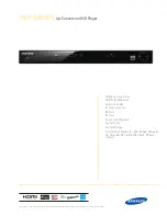
background image

FILE NO.

DVD-DX500

(Product Code: 1 682 340 51)
(Australia, New Zealand)

DVD-DX510

(Product Code: 1 682 340 52)
(Australia, New Zealand)
(Product Code: 1 682 342 82)
(India)

SERVICE MANUAL

SPECIFICATIONS

REFERENCE No. SM0905003

Power Source: 100-240V~, 50/60Hz
Power Consumption: 12W
Dimensions: 430(W) x 38(H) x 245(D)mm
Net Weight: Approx. 2.2kg

Specifications subject to change without notice.
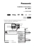
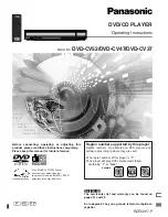
DVD Player 

DVR-DX500.indd   01

DVR-DX500.indd   01

2006/10/30   9:54:29

2006/10/30   9:54:29

All manuals and user guides at all-guides.com

all-guides.com

Summary of Contents for 1 682 340 51

Page 1: ... Product Code 1 682 342 82 India SERVICE MANUAL SPECIFICATIONS REFERENCE No SM0905003 Power Source 100 240V 50 60Hz Power Consumption 12W Dimensions 430 W x 38 H x 245 D mm Net Weight Approx 2 2kg Specifications subject to change without notice DVD Player All manuals and user guides at all guides com a l l g u i d e s c o m ...

Page 2: ...SPECIFICATIONS 2 3 CIRCUIT DIAGRAM INSTRUMENT DISASSEMBL PACKING VIEW Y 12 13 1 CONTENTS All manuals and user guides at all guides com ...

Page 3: ...uma 1 0 0 1Vp pChromaticity Color 0 286 20 Loadimpedance 75 Component Y 1Vp p Pb Pr 0 7Vp p Loadimpedance 75 Power 100 240V 50Hz 60Hz 12W Dimensiones Body W x Hx D 430 x 38 x 245 mm Packing 515 x 95 x 325 mm Weight Gross Net 2 9Kg 2 2Kg Notes Design and speci cations in this instruction manual are subjected to change with out prior notice toimprove quality and function DVD Audio output standards O...

Page 4: ...3 1 POWER SUPPLY SCHEMATIC DIAGRAM CIRCUIT DIAGRAM All manuals and user guides at all guides com ...

Page 5: ...4 2 DECODE BOARD SCHEMATIC DIAGRAM 1 INDEX SCHEMATIC DIAGRAM CIRCUIT DIAGRAM All manuals and user guides at all guides com ...

Page 6: ...5 2 RF MPEG SCHEMATIC DIAGRAM CIRCUIT DIAGRAM All manuals and user guides at all guides com a l l g u i d e s c o m ...

Page 7: ...6 3 SDRAM FLASH SCHEMATIC DIAGRAM CIRCUIT DIAGRAM All manuals and user guides at all guides com ...

Page 8: ...7 4 VIDEO OUTPUT PORT SCHEMATIC DIAGRAM CIRCUIT DIAGRAM All manuals and user guides at all guides com ...

Page 9: ...8 5 AUDIO OUTPUT PORT SCHEMATIC DIAGRAM CIRCUIT DIAGRAM All manuals and user guides at all guides com ...

Page 10: ...9 3 CONTROL BOARD SCHEMATIC DIAGRAM CIRCUIT DIAGRAM All manuals and user guides at all guides com ...

Page 11: ...R 0 3 C V 6 1 F U 0 1 9 1 C P 0 0 1 K 3 3 5 2 R 1 R k 7 4 7 2 R K 0 0 1 K 0 1 9 1 R 5 1 C V 0 5 F U 3 3 9 2 C 3 0 1 1 2 1 C V 5 2 F U 2 2 3 2 C U 1 0 2 1 C 3 2 2 9 2 R K 0 1 2 2 2 7 C 3 1 C 3 2 2 1 L B F 0 2 6 8 R 2 L B F P 0 0 1 5 2 C 4 C K 4 0 1 1 N C P 4 S N C 1 2 3 4 1 Q 5 1 8 1 C S 2 1 2 3 B C E 8 1 C V 0 5 F U 7 4 K 0 0 1 4 2 R 1 3 R K 7 4 4 1 C 3 0 1 0 2 6 4 R 7 2 C P 0 0 1 2 R V K 0 2 A 1 ...

Page 12: ...11 5 YUV BOARD SCHEMATIC DIAGRAM CIRCUIT DIAGRAM All manuals and user guides at all guides com ...

Page 13: ...2 1 Ass Y 8 MPEG PCB DW 15700340 1 Ass Y 2 0ch DVD DX500 only DW 15700290 1 Ass Y 5 1ch DVD DX510 only 9 BOTTOM COVER DW 13010147 1 SECC 10 YUV PCB DW 15760021 1 Ass Y When you order spare parts with the mark to our service team please inform them on PART NO with your model s final destination such as DW 12000347 Australia Note 1 Only the parts in above list are used for repairing 2 Other parts ex...

Page 14: ...13 PACKING VIEW SANYO Electric Co Ltd Osaka Japan Oct 06 All manuals and user guides at all guides com ...

Reviews: