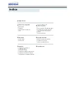
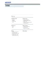
background image

Model:SC-148B

CONTENTS

CD-ROM

service 

manual

• Specifications

• Cautions at Service

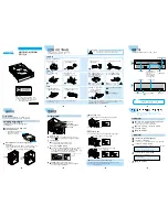
• External Part Name

• Disassembly Method

• Exploded Views & Part List

• Packing Options

• Operational Position Diagram

• Block Diagram

• Troubleshooting

• Circuit Diagram

• Main Components Block Diagram & Pin

Descriptions

• Electrical Parts List

The design and part of this product is subject to change without prior  notice for performance improvement.

Summary of Contents for SC-148B

Page 1: ...sembly Method Exploded Views Part List Packing Options Operational Position Diagram Block Diagram Troubleshooting Circuit Diagram Main Components Block Diagram Pin Descriptions Electrical Parts List The design and part of this product is subject to change without prior notice for performance improvement ...

Page 2: ... Samsung Electronics Co Ltd MAY 1999 Printed in Korea Code No BG68 00112A Electronics ...

Page 3: ... Impedance Below 104 It removes the electricity formed in body 2 Work table earthing Put the earthed conductive plate Impedance Below 104 such as copper plate on work table 3 Cautions for clothes Do not have any clothes touch with Pick up because the electricity formed in clothes is destroyed easily Cautions at Service 1 General Items 1 Be careful not to have your eyes or a part of body touch with...

Page 4: ...28 Main Components Block Diagram and Pin Descrition TA2143FN I C RF ...

Page 5: ...S ERROR SIGNAL GENERATING AMP OUTPUT TERMINAL 17 FEN FOCUS ERROR SIGNAL GENERATING AMP REVERSE INPUT TERMINAL 18 VDDIN VDD INPUT TERMINAL 19 VREF STANDARD VOLTAGE VREF OUTPUT TERMINAL VDDIN 3 6 V VREF 1 80 V 20 RFRP SIGNAL GENERATING AMP OUTPUT TERMINAL FOR TRACK COUNTER 21 BTC RECT SIGNAL GENERATING BOTTOM DETECTOR CONTROL TERMINAL 22 RFCT RFRP SIGNAL CENTER LEVEL OUTPUT TERMINAL 23 PKC RFCT SIGN...

Page 6: ...30 TC9450BF I C DSP ...

Page 7: ... XO MICOMCLOCKDRIVINGCIRCUITOUTPUTTERMINAL 25 TMAX TMAXDETECTIONRESULTOUTPUTTERMINAL 75 XVDD3 MICOMCLOCKDRIVINGCIRCUIT 3 3VPOWERTERMINAL 26 LPFN AMPREVERSEINPUTTERMINALFORLOW PASSFILTER 76 DVSS3 D ACONVERTRCHANNELANALOGGNDTERMINAL 27 LPFO AMPOUTPUTTERMINALFORLOW PASSFILTER 77 RO RCHANNELDATAOUTPUTTERMINAL 28 PVREF VREF 1 65V FORPLLONLY 78 DVDD3 DIGITAL ANALOGCONVERT 3 3VPOWERTERMINAL 29 VCOREF VCO...

Page 8: ...32 KS88C4504 12 I C MICOM ...

Page 9: ...D2 I EXT PROM DATA2 20 P4 1 BUS1 I O DSP COMMAND BUS1 60 D3 D3 I EXT PROM DATA3 21 P4 0 BUS0 I O DSP COMMAND BUS0 61 D4 D4 I EXT PROM DATA4 22 PWM1 PWM1 O PWM CONTROL 62 D5 D5 I EXT PROM DATA5 23 PWM0 PWM0 O PWM CONTROL 63 D6 D6 I EXT PROM DATA6 24 P3 5 CENT O DRIVE IC RESET 64 D7 D7 I EXT PROM DATA7 25 P3 4 CENT O CENTER SERVO CONTROL 65 A0 A0 O EXT PROM ADDRESS 0 26 P3 3 SPM_FG I SPINDLE MOTOR C...

Page 10: ...34 TC9474FA I C DECODER ...

Page 11: ...GROUND TERMINAL 75 AZCK BASE CLOCK INPUT ON FAST PLAY 26 HD1 HOST DATA INPUT 76 SBSY SUBCODE BLOCK SYNC OUTPUT 27 HD14 HOST DATA INPUT 77 SFSY SUBCODE DATA SYNC FRAME INPUT 28 HD0 HOST DATA INPUT 78 SBDI SUBCODE DATA INPUT 29 HD15 HOST DATA INPUT 79 CLCK SUBCODE DATA CLOCK OUTPUT 30 VSS GROUND TERMINAL 80 C2PI DATA CORRECTION FLAG INPUT 31 HDRQ DATA REQUEST TERMINAL 81 LRCK CHANNEL CLOCK INPUT 32 ...

Page 12: ...36 TA8493AF I C DRIVE ...

Page 13: ...37 7S32 I C OR GATE 4S66F I C SWITCH PQ20WZ51 I C REGULATOR DAP202K DIODE ARRAY Pin No Pin Name DC input VIN ON OFF control terminal VC DC output VO Output voltage minute adjustment terminal VADJ GND ...

Page 14: ...7 DQ0 Data Input output To output data during read cycles and receive input data during write cycles Data is internally latched during a write cycle The outputs are in tri state when OE or CE is high OE Chip Enable To activate the device when CE is low OE Output Enable To gate the data output buffers WE Write Enable To control the write operations Vcc Power Supply To provide 5 volt supply 10 Vss G...

Page 15: ...ed output VM2 CH2 inverted output VM4 CH4 non inverted output VM2 CH2 non inverted output VM4 CH4 inverted output VM1 CH1non inverted output VM5 CH5 non inverted output VM1 CH1 inverted output VM5 CH5 inverted output OUT1 E1 amplifier ouptut OUT5 E5 amplifier output IN1 E1 amplifier inverted input IN5 E5 amplifier inverted input Vm1 Motor power supply IN5 E5 amplifier non inverted input VBS1 Boots...

Page 16: ...al input Connect to hall element output terminal terminal 16 Hc c phase positive hall signal input Connect to hall element output terminal terminal 17 Hc a phase negative hall signal input Connect to hall element output terminal terminal 18 HB Hall element bias terminal Open collector output Connect to the negative side of hall element bias line 19 Cd Forward reverse changeover gain Adjust a rotat...

Page 17: ... from 0V to 5V Inputted Voltage of IC301 5pin is 1 5V 2 0V Check R401 R402 R333 Rsoldering Y Y N N N N N Input output IC301 57pi n 80pin 1pin 4pin pulse waveform Check IC301 pin soldering Y Y Y N In case FLASH ROM Memory of IC301 16pin 0V and Rom memory inputted 5V Check R320 R321 soldering Check R301 R302 soldering Equipments required at repair 1 Oscilloscope 100MHz or more 2 PROBE for Oscillosco...

Page 18: ... diode on Refer to No focus lock Y Focuse up down Y Disc rotates Refer to No disc rotation Y Pause state Pause state LED off as disc rotation state and continue 1 track jump Y Spindle lock Y Input Voltage of IC201 9pin 21pin 3 6V Pick up moves in at power on after moving out Check after SET assembly 1TRACK JUMP TE A ...

Page 19: ...y in CN702 4pin becomes 0V CN702 2pin becomes 0V N N N N IC301 28pin is 0V with tray open Check R502 R503 R509 soldering CheckIC301 33pin 34pin soldering Check R502 R503 soldering CheckIC301 33pin 34pin soldering Replace IC501 Replace IC501 Y Y Y Y IC501 11pin change from 1 75V to 0V at pressing SW702 N N N N N IC301 33pin changes from 1 75V to 5V at pressing SW702 IC501 13pin changes from 2 4V to...

Page 20: ... and initial state N N IC101 9pin changes from 4 2V to 3 6V Check IC101 power input and replace Y Open and close tray Disc insettion Y CN501 3pin changes from 2V to 2 5V Check D101 L101 Q102 R102 C103 soldering Y CN501 2pin changes from 0V to 0 7V Check Pick up FPC connection state N N N Y Replace pick up Y ...

Page 21: ...ed in IC301 22Pin 23pin N Refer to Check power source and initial state N Voltage of IC501 4pin 12V 5pin 5V Check R506 R507 R512 soldering After checking IC501 soldering no error replace IC N Y N N The below signal is inputted in CN503 A A B B termial Y The opposition signal is inputted in CN503 A A B B termial Y Replace SLED Motor Y ...

Page 22: ...3pin soldering N Check IC301 38pin soldering Check R323 soldering The below waveform is inputted in IC502 22Pin IC502 4Pin 29pin is 12V Insert disc Y Y Y Y Y Y Y Y Spindle motor kick signal IC502 5Pin is 5V Replace IC502 Spindle Motor FPC is connected Replace spindle Motor IC502 5Pin is 5V The below waveform is inputted in IC502 Y ...

Page 23: ...o Spindle Motor rotation N Y Audio signal is outputted in IC201 77 80Pin Check IC201 power and soldering N Replace IC201 N Y Audio signal is outputted in IC701 1 7Pin Check IC701 power input and peripheral integer VR soldering N Replace IC701 N Y Audio signal is outputted in JK 701 Check L702 L701 soldering N ...

Page 24: ...tion pattern change from 0V to 5V Check the soldering of IC401 IC301 and pattern open short N N Y Y IC401 CN701 is normal communication singnds Check the soldering of Damping Resister and IC I F Wafer N Connet 1 F cable Y Is IC301 55PIN 5V when main power turns on Check main power end and initial state N Does X401 oscillate Check soldering of C401 C402 Y Y Is IC201 95PIN 5V N Y ...

Page 25: ... from 0V to 5V Inputted Voltage of IC301 5pin is 1 5V 2 0V Check R401 R402 R333 Rsoldering Y Y N N N N N Input output IC301 57pi n 80pin 1pin 4pin pulse waveform Check IC301 pin soldering Y Y Y N In case FLASH ROM Memory of IC301 16pin 0V and Rom memory inputted 5V Check R320 R321 soldering Check R301 R302 soldering Equipments required at repair 1 Oscilloscope 100MHz or more 2 PROBE for Oscillosco...

Page 26: ... diode on Refer to No focus lock Y Focuse up down Y Disc rotates Refer to No disc rotation Y Pause state Pause state LED off as disc rotation state and continue 1 track jump Y Spindle lock Y Input Voltage of IC201 9pin 21pin 3 6V Pick up moves in at power on after moving out Check after SET assembly 1TRACK JUMP TE A ...

Page 27: ...y in CN702 4pin becomes 0V CN702 2pin becomes 0V N N N N IC301 28pin is 0V with tray open Check R502 R503 R509 soldering CheckIC301 33pin 34pin soldering Check R502 R503 soldering CheckIC301 33pin 34pin soldering Replace IC501 Replace IC501 Y Y Y Y IC501 11pin change from 1 75V to 0V at pressing SW702 N N N N N IC301 33pin changes from 1 75V to 5V at pressing SW702 IC501 13pin changes from 2 4V to...

Page 28: ... and initial state N N IC101 9pin changes from 4 2V to 3 6V Check IC101 power input and replace Y Open and close tray Disc insettion Y CN501 3pin changes from 2V to 2 5V Check D101 L101 Q102 R102 C103 soldering Y CN501 2pin changes from 0V to 0 7V Check Pick up FPC connection state N N N Y Replace pick up Y ...

Page 29: ...ed in IC301 22Pin 23pin N Refer to Check power source and initial state N Voltage of IC501 4pin 12V 5pin 5V Check R506 R507 R512 soldering After checking IC501 soldering no error replace IC N Y N N The below signal is inputted in CN503 A A B B termial Y The opposition signal is inputted in CN503 A A B B termial Y Replace SLED Motor Y ...

Page 30: ...3pin soldering N Check IC301 38pin soldering Check R323 soldering The below waveform is inputted in IC502 22Pin IC502 4Pin 29pin is 12V Insert disc Y Y Y Y Y Y Y Y Spindle motor kick signal IC502 5Pin is 5V Replace IC502 Spindle Motor FPC is connected Replace spindle Motor IC502 5Pin is 5V The below waveform is inputted in IC502 Y ...

Page 31: ...o Spindle Motor rotation N Y Audio signal is outputted in IC201 77 80Pin Check IC201 power and soldering N Replace IC201 N Y Audio signal is outputted in IC701 1 7Pin Check IC701 power input and peripheral integer VR soldering N Replace IC701 N Y Audio signal is outputted in JK 701 Check L702 L701 soldering N ...

Page 32: ...tion pattern change from 0V to 5V Check the soldering of IC401 IC301 and pattern open short N N Y Y IC401 CN701 is normal communication singnds Check the soldering of Damping Resister and IC I F Wafer N Connet 1 F cable Y Is IC301 55PIN 5V when main power turns on Check main power end and initial state N Does X401 oscillate Check soldering of C401 C402 Y Y Is IC201 95PIN 5V N Y ...

Page 33: ...Part Name 1 Front 2 Rear Earphone jack Digital output terminal Optional Sound output terminal Interface terminal Master Slave select pin Power terminal Up Down Volume LED Stop Open button Emergency HOLE Disc tray ...

Page 34: ...ER BOTTOM ASSY as shown in the figure of the next page 2 COVER TOP disassembly After disassembling 6 hooks of FRONT ASSY 29 from COVER TOP 30 pull COVER TOP 30 forward and disassemble it 3 ASSY DECK PCB MAIN disassembly Disassemble FPC PICK UP 24 and FPC MOTOR 25 connected between assy deck and PCB main then disassemble between deck and PCB main ...

Page 35: ...4 Exploded Views ...

Page 36: ... 00071A TURN TABLE ABS AL BG66 00010A BRKT T T SECC 1 0T BG61 00018A COVER T T SUS 0 3T BG63 30018A BALL TURN TABLE NI TRONIC BG70 10316A RUBBER T T CR 0 45T Ø28 21 BG73 10107A SCREW SP MOTOR M1 7 3 BG60 10020A ASSY FEEDING BG97 00021A 19 CHASSIS SUB ABS PC BG61 00001A 15 MAIN BASE M OUTSERT BG61 00002A SECC 1 6T BG61 00004A 20 RUBBER INSULATOR BUTYL BG73 00001A SCREW TAPPING AH60 10143A 21 FFC SP...

Page 37: ...69 20327A BG69 30305A BG46 30001J BG39 42001A BG69 30307A BG68 00043A BG39 30002A PARTS PACKING CASE CUSHION SET BAG PE DISC FLOPPY CABLE WIRE HARNESS PE BAG MANUAL USERS CABLE IF SPECIFICATION SW 1E EPS LDPE 3 5 INCH 4P LDPE 380MM Q TY 1 2 1 1 1 1 1 1 REMAR K ...

Page 38: ... C517 C522 C524 C117 C211 C106 C113 C213 C221 C116 C308 C312 C314 C602 C606 C607 4 2203 000257 C503 C306 6 103 C202 C203 C224 C609 5 2203 000560 C112 2 224 C111 6 2203 000919 C210 1 474 7 2203 000626 C408 3 22P C207 C208 8 2203 000715 C204 C216 C219 3 332 9 2203 000783 C201 1 331 10 2203 000815 C110 1 33P 11 2203 001052 C206 1 561 12 2203 001195 C303 C304 2 7P 13 2203 001607 C519 2 221 C511 14 220...

Page 39: ...527 R717 R718 12 2007 000092 R301 R503 2 15K 13 2007 000094 R112 R113 R276 R277 R278 6 22K R502 14 2007 000097 R441 R336 R323 10 47K R104 R105 R110 R111 R114 R116 R435 15 2007 000098 R531 R533 2 56K 16 2007 000100 R507 R510 R511 R512 4 68K 17 2007 000102 R319 R504 R506 R514 R529 11 100K R532 R337 R271 R304 R305 R321 18 2007 000109 R210 2 1M 19 2007 000122 R436 1 1 2K 20 2007 000123 R715 R720 2 1 5...

Page 40: ... B601 B602 B603 B604 4 BEAD 6 3704 000249 IC306S 1 SOCKET IC 7 3708 001346 CN702 1 13PIN 8 3708 001347 CN503 1 4PIN 9 3708 001348 CN502 1 11PIN 10 3708 001380 CN501 1 17PIN 11 3711 003262 CN701 1 5IN1 12 0407 000116 D101 1 DAP202K 13 0501 000251 Q102 Q501 2 BC807 14 0501 000534 Q702 Q703 2 2SC2412K 15 0501 000150 Q701 1 2SA1037 16 BG41 00018A PCB 0 25 PCB 43 ...

Page 41: ... ROM 9 3722 001338 JK701 1 JACK DC POWER 6P 3C 3 6mm SN BLK NO 10 3301 001015 L701 L702 2 CORE FERRITE BEAD 11 2001 000380 R701 R702 2 R CARBON 160KOHM 5 1 8W AA TP 1 8X3 2MM 12 2001 000515 R703 1 R CARBON 220OHM 5 1 8W AA TP 1 8X3 2MM 13 2001 000281 R704 1 R CARBON 100OHM 5 1 8W AA TP 1 8X3 2MM 14 2001 000281 R705 R CARBON 100OHM 5 1 8W AA TP 1 8X3 2MM 15 2001 000745 R707 1 R CARBON 4 7OHM 5 1 8W...

Page 42: ...17 Block Diagram ...

Page 43: ...17 Block Diagram ...

Page 44: ...7 Operational Position Diagram ...

Page 45: ...Operational Position Diagram 8 ...

Page 46: ...9 Operational Position Diagram ...

Page 47: ...Operational Position Diagram 10 ...

Page 48: ...11 Operational Position Diagram ...

Page 49: ...Operational Position Diagram 12 ...

Page 50: ...13 Operational Position Diagram ...

Page 51: ...Operational Position Diagram 14 ...

Page 52: ...15 Operational Position Diagram ...

Page 53: ...16 Operational Position Diagram ...

Page 54: ...26 ...

Page 55: ...27 Circuit Diagram ...

Reviews: