Samsung S3F84B8, User Manual
The Samsung S3F84B8 user manual is available for free download on our website. This comprehensive manual provides detailed instructions, troubleshooting tips, and useful information to enhance your experience with this outstanding product. Get the most out of your Samsung S3F84B8 by downloading the user manual from manualshive.com.
Share
Download


Reviews:
No comments
Related manuals for S3F84B8
MR Series
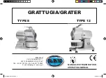
Brand: FABIO LEONARDI Pages: 20
Elegant
Brand: Xavax Pages: 2
G2
Brand: La Monferrina Pages: 58
Cooktop
Brand: Keating Of Chicago Pages: 16
VP800
Brand: Vacmaster Pages: 24
FS1000
Brand: Waring Pages: 12
8115
Brand: OBH Nordica Pages: 16
CT 100
Brand: Bartscher Pages: 15
508
Brand: BALAY Pages: 31
25460
Brand: Hamilton Beach Pages: 2
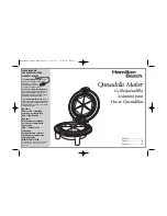
25409
Brand: Hamilton Beach Pages: 40
8
Brand: R.G.V. Pages: 24
CSIG 501
Brand: Parkinson Cowan Pages: 52
840167000
Brand: GE Pages: 16
106810
Brand: GE Pages: 7
Monogram ZDBT240
Brand: GE Pages: 8
Profile TRATTORIA PS96PZRSS
Brand: GE Pages: 12
Groen Tri-Res20
Brand: Groen Pages: 6


