
©
Samsung Electronics Co., Ltd. Aug. 1996.
Code No. AH68-20128A
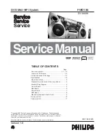
MICRO COMPONENT SYSTEM
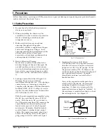
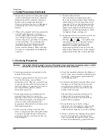
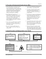
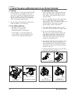
1. Precautions
2. Specifications
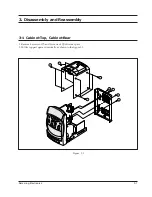
3. Disassembly and Reassembly
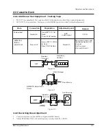
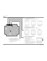
4. Alignment and Adjustments
5. Special Circuit Descriptions
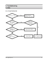
6. Troubleshooting
7. Exploded Views and Parts List
8. Electrical Parts List
9. Block Diagrams
10. PCB Diagrams
11. Wiring Diagram
12. Schematic Diagrams
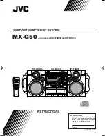
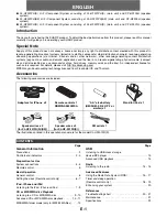
POWER
SUPER BASS
VOLUME
DOWN UP
ON/STANDBY
CD REPEAT A
↔
B
PHONEG
EQ PRESET
TAPE
CD
BAND
TUNER
AUX
TUNING
SERVICE
Manual
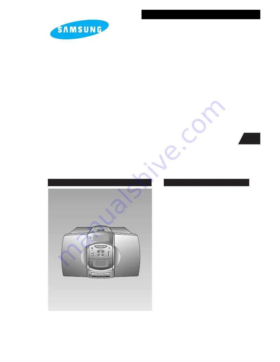
MICRO COMPONENT
SYSTEM
MM-16
CONTENTS
Summary of Contents for MM-16
Page 24: ...Samsung Electronics 7 5 Exploded Views and Parts List 7 3 1 CD DECK Exploded View ...
Page 40: ...Block Diagrams KS9282 DSP NIC9282 9 8 Samsung Electronics ...
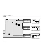
Page 43: ...10 PCB Diagrams 10 1 Main 10 1 Samsung Electronics ...
Page 44: ...Samsung Electronics 10 2 10 2 Front PCB Diagrams ...
Page 45: ...10 3 Samsung Electronics 10 3 CD 10 3 1 Top View 10 3 2 Bottom View PCB Diagrams ...