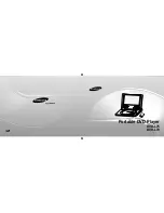
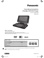
background image

PORTABLE DVD PLAYER

DVD-L200W
DVD-L200

SERVICE 

1. Precautions

2. Troubleshooting

3. Exploded Views and Parts List

4. Electrical Parts List

5. Block Diagram

6. Schematic Diagrams

Manual 

PORTABLE DVD PLAYER

CONTENTS

SERVICE MANUAL

DVD-L200W/DVD-L200

ELECTRONICS

© Samsung Electronics Co., Ltd. 

SEP. 2003

Printed in Korea

AK82-00404A

This Service Manual is a property of Samsung Electronics Co .,Ltd.
Any unauthorized use of Manual can be punished under applicable

International and/or domestic law.

Summary of Contents for DVD-L200

Page 1: ...ock Diagram 6 Schematic Diagrams Manual PORTABLE DVD PLAYER CONTENTS SERVICE MANUAL DVD L200W DVD L200 ELECTRONICS Samsung Electronics Co Ltd SEP 2003 Printed in Korea AK82 00404A This Service Manual is a property of Samsung Electronics Co Ltd Any unauthorized use of Manual can be punished under applicable International and or domestic law ...

Page 2: ...erwriters Laboratories UL 1270 40 7 With the instrument s AC switch first in the ON position and then in the OFF position measure from a known earth ground metal water pipe conduit etc to all exposed metal parts of the instrument antennas handle brackets metal cabinets screw heads metallic overlays control shafts etc espe cially any exposed metal parts that offer an electri cal return path to the ...

Page 3: ...nched out of place or frayed wiring Do not change spacing between a component and the printed circuit board Check the AC power cord for damage 5 Components parts and or wiring that appear to have overheated or that are otherwise damaged should be replaced with components parts and or wiring that meet original specifications Additionally determine the cause of overheating and or damage and if neces...

Page 4: ...d lead last 2 The service precautions are indicated or printed on the cabinet chassis or components When servic ing follow the printed or indicated service precau tions and service materials 3 The components used in the unit have a specified flame resistance and dielectric strength When replacing components use components which have the same ratings Components identi fied by shading by or by in th...

Page 5: ...posure of the assem bly 3 Use only a grounded tip soldering iron to solder or unsolder ESD devices 4 Use only an anti static solder removal devices Some solder removal devices not classified as anti static can generate electrical charges suffi cient to damage ESD devices 5 Do not use freon propelled chemicals These can generate electrical charges sufficient to damage ESD devices 6 Do not remove a ...

Page 6: ... sheet This gives them the same ground as the sheet 4 Remove the optical pick up block 5 Perform work on top of the conductive sheet Be careful not to let your clothes or any other static sources to touch the unit Be sure to put on a wrist strap grounded to the sheet Be sure to lay a conductive sheet made of copper etc Which is grounded to the table Fig 1 3 6 Short the short terminal on the PCB wh...

Page 7: ...solder land 3 points short on Pick up FPC See Fig 1 4 4 Disassemble the Pick up 1 5 2 Assembly 1 Replace the Pick up 2 Remove the soldering 3 points on Pick up FPC 3 Reassemble the Ass y DVD Deck ASS Y DVD DECK FPC Bottom View SOLDER LAND 3 POINTS SHORT Note If the assembly and disassembly are not done in correct sequence the Pick up may be damaged Fig 1 4 ...

Page 8: ...ithin specified range Check Deck Ass y Check RIC1 and A B C D input Yes No A Samsung Electronics 2 1 2 Troubleshooting No Disc recognition LD is outputted from object lens at play key input No focus incoming and no disc occurs Yes No B A ...

Page 9: ...xceeds 0 1A LD out pick up replace Open check in related circuit Check SIC1 Yes Yes Yes No No Divide RQ1 emitter terminal voltage and 5V real voltage difference into 6 2ohm B No pick up home positing SIC1 13output is normal Check the Deck Ass y and connection Check SIC1 Yes No ...

Page 10: ...jump counts Check SIC1 peripheral circuit SIC1 3 output is normal Check Deck Ass y Check Deck Ass y Check RIC1 31 terminal Yes Yes Yes Yes Yes Yes No No No No No No No Search Operation TEZISLV SIC1 6 output is normal Actual velocity occurs at SIC1 13 terminal Check RIC1 peripheral circuit RFAGCO RIC1 71 output level is normal Check SIC1 peripheral circuit No No No Yes TE occurs in search range Foc...

Page 11: ...IC185 peripheral circuit Yes No Output in AIC02 AIC02 8 9 is normal Check AIC02 1 2 16 function select Yes No Abnormal rotation of disc motor Input of RF signal is normal SIC1 152 SPD output is normal SIC1 28 After resoldering SIC1 SIC3 7 output FG is normal Check or replace disc motor or check SIC1 MIC1 Check Deck ass y and connection Check path to RIC1 and SIC1 Check RIC1 soldering and power RIC...

Page 12: ... is normal Check Jack3 peripheral soldering shot Check ZIC01 peripheral circuit Check Jack3 Yes No No Yes Headphone output error Jack1 Jack2 output is normal AIC06 AIC07 1 5 output is normal Check Jack1 Jack2 peripheral soldering shot Check Jack1 Jack2 output error Check AIC02 AIC03 4 output Yes No No Yes ...

Page 13: ...and pin6 2 in VIC01 Check the connection betwen VIC01 and pin 4 in PQ118 Check the soldering of VIC01 No Check the connection between VIC01 and output jack Pin of DAC VDD in ZIC1 has normal level Check the connection to positive pin in PE120 Yes No Peak to peak voltage level of VR101 102 Y and C signal appears at output jack at pin5 4 No Yes Check the cable Speater output error AIC05 5 8 14 18 out...

Page 14: ...pin4 in PIC03 and pin30 in UIC01 Yes No Yes 8 38MHz is normal at pin40 41 in UIC01 No Yes Change UXT02 Check the battery CVBS output error 27MHz clock input is normal at pin 161 in ZIC1 Analog output is normal at pin 169 in ZIC1 Check the connection between pin 161 in ZIC1 and ZX101 Check the soldering of ZIC1 Yes No No Analog signals are inputted normally at pin4 in VIC01 Yes No Power is normal a...

Page 15: ...t 32KHz output is normal at pin77 in XIC01 Yes Check the connection between pin4 5 in XCON1 and pin4 in XQ102 About 27MHz clock input is normal at pin2 in XIC01 Check the soldering of XIC01 No VDD appears at pin36 in XCON1 Check the connection between pin36 in XCON15 and PF501 Yes No Yes 13 5MHz input is normal at pin93 in XIC01 No Pin of VDD_3 3 VDD_2 5 in XIC01 has normal level Yes Check the con...

Page 16: ...3 1 3 Exploded View and Parts List 3 1 Cabinet Assembly 3 2 Deck Assembly Page 3 2 3 4 You can search for the updated part code through ITSELF web site URL http itself sec samsung co kr Notice ...

Page 17: ...Exploded Views and Parts List 3 2 3 1 Cabinet Assembly UT01 U Q 1 E 3 2 5 w 4 6 e 0 q 0 8 8 8 8 8 8 9 7 7 H100 r MAIN B PCB R MAIN A PCB T KEY PCB t TERMINAL PCB Y y ...

Page 18: ... NI PLT 19 AH64 02398A WINDOW REMOCON DVD L200 ACRYL 20 AH64 02487A INDICATOR LED DVD L200 PMMA DVD 21 AC60 10024A SCREW MACHINE FZW FE M2 X3 22 6001 001533 SCREW MACHINE PH M2 0 L4 0 CR PLT SWRC 23 AH69 00667B CUSHION LCD DVD L100 PORON T1 24 AK66 00005A SHAFT DISC DVD L100 SUS OD1 8 25 AH61 01102A SPRING ETC COVER DVD L100 SUS 304 26 AH61 01322A FRAME HOUSING DVD L200 SPTE T0 5 28 AH66 00224A LE...

Page 19: ...Exploded Views and Parts List 3 4 3 2 Deck Assembly H115 H101 H103 H112 H116 H102 H116 H116 H105 H106 H107 H111 H115 H104 H117 H113 H114 H109 H104 H104 S N A H110 H116 H108 ...

Page 20: ...7 AK97 00320A ASSY LEAD SCREW PORTABLE2 H108 AK66 00020A SHAFT PU DP P2 SUS420J2 H109 AK97 00312A ASSY PICK UP SOH DPS ASSY PICK UP H110 AK31 00007A MOTOR BLOWER SPINDLE DP P2 H111 AK61 00074A SPRING ETC SHAFT PU DP 7 SUS304 CSP H112 AK61 00079A SPRING ETC SHAFT LEAD SCREW DP P2 SUS304 H113 AK61 00082A SPRING ETC PU DP P2 SUS304 CSP H114 AK61 00078A SPRING ETC PU NUT DP P2 SUS304 CSP H115 6001 001...

Page 21: ...Exploded Views and Parts List 3 6 MEMO ...

Page 22: ...404 000256 C TA CHIP 47UF 20 16V GP TP 7343 AE155 2404 000299 C TA CHIP 22uF 20 16V TP 6032 AE165 2404 001001 C TA CHIP 10uF 10 6 3V GP TP 3216 3 2mm AE166 2404 000299 C TA CHIP 22uF 20 16V TP 6032 AE167 2404 001001 C TA CHIP 10uF 10 6 3V GP TP 3216 3 2mm AE171 2404 001043 C TA CHIP 47uF 20 10V GP TP 6032 AE176 2404 000259 C TA CHIP 47uF 20 6 3V TP 6032 AE177 2404 000259 C TA CHIP 47uF 20 6 3V TP ...

Page 23: ... FE2 2404 001043 C TA CHIP 47uF 20 10V GP TP 6032 FE3 2404 001043 C TA CHIP 47uF 20 10V GP TP 6032 FE4 2404 001043 C TA CHIP 47uF 20 10V GP TP 6032 FE5 2404 001043 C TA CHIP 47uF 20 10V GP TP 6032 FE6 2404 001001 C TA CHIP 10uF 10 6 3V GP TP 3216 3 2mm FL1 2703 000398 INDUCTOR SMD 10uH 10 3225 FR1 2007 000084 R CHIP 4 7Kohm 5 1 10W TP 1608 FR10 2007 000092 R CHIP 15Kohm 5 1 10W TP 1608 FR15 2007 0...

Page 24: ...07 000077 R CHIP 470ohm 5 1 10W TP 1608 RR9 2007 000312 R CHIP 10ohm 5 1 4W TP 3216 SC1 2203 005148 C CER CHIP 100nF 10 16V X7R TP 1608 SC101 2203 005148 C CER CHIP 100nF 10 16V X7R TP 1608 SC102 2203 005148 C CER CHIP 100nF 10 16V X7R TP 1608 SC103 2203 000552 C CER CHIP 0 02NF 5 50V C0G TP 1608 SC104 2203 000552 C CER CHIP 0 02NF 5 50V C0G TP 1608 SC106 2203 000257 C CER CHIP 10nF 10 50V X7R TP ...

Page 25: ...TP 1608 SR44 2007 000084 R CHIP 4 7Kohm 5 1 10W TP 1608 SR45 2007 000102 R CHIP 100Kohm 5 1 10W TP 1608 SR48 2007 000070 R CHIP 0ohm 5 1 10W TP 1608 SR49 2007 000305 R CHIP 10Mohm 5 1 10W TP 1608 SR5 2007 000091 R CHIP 12Kohm 5 1 10W TP 1608 SR50 2007 000305 R CHIP 10Mohm 5 1 10W TP 1608 SR52 2007 000070 R CHIP 0ohm 5 1 10W TP 1608 SR54 2007 000070 R CHIP 0ohm 5 1 10W TP 1608 SR6 2007 000070 R CHI...

Page 26: ...7R TP 1608 ZC102 2203 005148 C CER CHIP 100nF 10 16V X7R TP 1608 ZC103 2203 005148 C CER CHIP 100nF 10 16V X7R TP 1608 ZC104 2203 005148 C CER CHIP 100nF 10 16V X7R TP 1608 ZC105 2203 005148 C CER CHIP 100nF 10 16V X7R TP 1608 ZC106 2203 005148 C CER CHIP 100nF 10 16V X7R TP 1608 ZC107 2203 005148 C CER CHIP 100nF 10 16V X7R TP 1608 ZC109 2203 005148 C CER CHIP 100nF 10 16V X7R TP 1608 ZC11 2203 0...

Page 27: ...P 1608 AR214 2007 000074 R CHIP 100ohm 5 1 10W TP 1608 AR215 2007 000074 R CHIP 100ohm 5 1 10W TP 1608 AR216 2007 000078 R CHIP 1Kohm 5 1 10W TP 1608 AR218 2007 000078 R CHIP 1Kohm 5 1 10W TP 1608 AR219 2007 000078 R CHIP 1Kohm 5 1 10W TP 1608 AR233 2007 000107 R CHIP 470Kohm 5 1 10W TP 1608 AR234 2007 000107 R CHIP 470Kohm 5 1 10W TP 1608 AR235 2007 000078 R CHIP 1Kohm 5 1 10W TP 1608 AR236 2007 ...

Page 28: ...CHIP 4 7Kohm 5 1 10W TP 1608 PR133 2007 000092 R CHIP 15Kohm 5 1 10W TP 1608 PR134 2007 000097 R CHIP 47Kohm 5 1 10W TP 1608 PR135 2007 000094 R CHIP 22Kohm 5 1 10W TP 1608 PR136 2007 000094 R CHIP 22Kohm 5 1 10W TP 1608 PR137 2007 000091 R CHIP 12Kohm 5 1 10W TP 1608 PR138 2007 000086 R CHIP 5 6Kohm 5 1 10W TP 1608 PR139 2007 000097 R CHIP 47Kohm 5 1 10W TP 1608 PR140 2007 000091 R CHIP 12Kohm 5 ...

Page 29: ... CHIP 0ohm 5 1 10W TP 1608 UR301 2007 000070 R CHIP 0ohm 5 1 10W TP 1608 UR302 2007 000070 R CHIP 0ohm 5 1 10W TP 1608 USW01 3404 001121 SWITCH TACT 12V DC 50mA 160gf 4 8x4 8x0 USW02 3404 001121 SWITCH TACT 12V DC 50mA 160gf 4 8x4 8x0 USW03 3404 001121 SWITCH TACT 12V DC 50mA 160gf 4 8x4 8x0 USW04 3404 001121 SWITCH TACT 12V DC 50mA 160gf 4 8x4 8x0 USW05 3404 001121 SWITCH TACT 12V DC 50mA 160gf 4...

Page 30: ...16 2007 001433 R CHIP 12Kohm 1 1 10W TP 1608 R17 2007 000842 R CHIP 3Kohm 1 1 10W TP 1608 R19 2007 001433 R CHIP 12Kohm 1 1 10W TP 1608 R20 2007 001153 R CHIP 750ohm 1 1 10W TP 1608 R21 2007 000857 R CHIP 4 3Kohm 1 1 10W TP 1608 R22 2007 000999 R CHIP 510ohm 1 1 10W TP 1608 R23 2007 000070 R CHIP 0ohm 5 1 10W TP 1608 R24 2007 000509 R CHIP 2 4Kohm 1 1 10W TP 1608 R27 2007 000640 R CHIP 270ohm 1 1 ...

Page 31: ...This Document can not be used without Samsung s authorization 4 10 Samsung Electronics Electrical Parts List MEMO ...

Page 32: ...ker R Speaker L UIC01 uPD78F0034AGK Front Micom L L R SCL SDA R Headphone 2 Headphone 1 AIC101 CS4391 DAC VIC01 MM1566 6dB Amp ZIC2 NT5SV4M16DT 64MBit SDRAM XTC02 03 74LVX573 MUX ZIC7 KS24CD20 EEPROM XTC01 Jag D Scaler SIC01 SAA7114 Video Decoder U1 LWT13611 Timing Controller AIC02 MPC509 MUX AIC05 TPA6017A Speaker Amp AIC06 TPA302 Headphone Amp AIC07 TPA302 Headphone Amp LCD Display ZIC3 29LV800B...

Page 33: ...Block Diagram 5 2 Samsung Electronics This Document can not be used without Samsung s authorization MEMO ...

Page 34: ...tic Diagrams 6 2 6 3 6 4 6 5 6 6 6 7 6 8 6 9 6 10 6 11 6 12 6 1 DCDC Battery Main B PCB 6 2 Power Main A PCB 6 3 AV Decoder Main A PCB 6 4 Servo Main A PCB 6 5 Video 1 Audio 2 Main B PCB 6 6 Video 2 Main A PCB 6 7 Audio 1 Main A PCB 6 8 Display Main A PCB 6 9 Key Sub Micom 6 10 LCD 6 11 Inverter ...

Page 35: ...Schematic Diagrams 6 2 Samsung Electronics This Document can not be used without Samsung s authorization 6 1 DCDC Battery Main B PCB ...

Page 36: ...6 2 Power Main A PCB Schematic Diagrams Samsung Electronics 6 3 This Document can not be used without Samsung s authorization ...

Page 37: ...Schematic Diagrams 6 4 Samsung Electronics This Document can not be used without Samsung s authorization 6 3 AV Decoder Main A PCB ...

Page 38: ...Schematic Diagrams Samsung Electronics 6 5 This Document can not be used without Samsung s authorization 6 4 Servo Main A PCB ...

Page 39: ...Schematic Diagrams 6 6 Samsung Electronics This Document can not be used without Samsung s authorization 6 5 Video 1 Audio 2 Main B PCB ...

Page 40: ...Schematic Diagrams Samsung Electronics 6 7 This Document can not be used without Samsung s authorization 6 6 Video 2 Main A PCB ...

Page 41: ...Schematic Diagrams 6 8 Samsung Electronics This Document can not be used without Samsung s authorization 6 7 Audio 1 Main A PCB ...

Page 42: ...Schematic Diagrams Samsung Electronics 6 9 This Document can not be used without Samsung s authorization 6 8 Display Main A PCB ...

Page 43: ...Schematic Diagrams 6 10 Samsung Electronics This Document can not be used without Samsung s authorization 6 9 Key Sub Micom ...

Page 44: ...Schematic Diagrams Samsung Electronics 6 11 This Document can not be used without Samsung s authorization 6 10 LCD ...

Page 45: ...Schematic Diagrams 6 12 Samsung Electronics This Document can not be used without Samsung s authorization 6 11 Inverter ...

Reviews: