


Television Video Cassette Recorder
Chassis :
V15A(REV.2)
Model :
CXJ1964BX/XAA
Television Video Cassette Recorder
CONTENTS
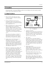
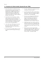
Precautions
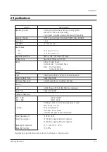
Specifications
Alignment and Adjustment (VCR)
Alignment and Adjustment (TV)
Timing Chart
Troubleshooting
Exploded View and Parts List
Electrical Parts List
Block Diagram
Wiring Diagram
Schematic Diagrams
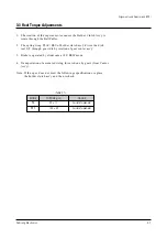
1.
2.
3.
4.
5.
6.
7.
8.
9.
10.
11.
Summary of Contents for CXJ1964BX/XAA
Page 2: ...ELECTRONICS Samsung Electronics Co Ltd DEC 2001 Printed in Korea 3V15A SMX 2045 ...
Page 8: ...2 2 Samsung Electronics MEMO ...
Page 18: ...MEMO 3 10 Samsung Electronics ...
Page 28: ...MEMO 4 10 Samsung Electronics ...
Page 30: ...MEMO 5 2 Samsung Electronics ...
Page 48: ...MEMO 6 18 Samsung Electronics ...
Page 61: ...8 10 Samsung Electronics MEMO ...
Page 62: ...9 Block Diagram Block Diagram Samsung Electronics 9 1 ...
Page 63: ...MEMO 9 2 Samsung Electronics ...
Page 66: ...PCB Layout Samsung Electronics 11 3 11 3 Main CONTROL ...
Page 67: ...10 Wiring Diagram Wiring Diagram Samsung Electronics 10 1 ...
Page 68: ...MEMO 10 2 Samsung Electronics ...
Page 71: ...Schematic Diagrams 11 3 Samsung Electronics 11 3 VCR POWER BLOCK ...