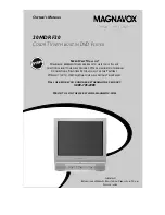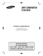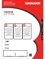


DVD Television
Chassis :
V18A
Model:
CFTD2083TX/SMS
DVD Television Cassette Recorder
CONTENTS
Precautions
Specifications
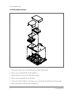
Disassembly and Reassembly
Alignment and Adjustment (Electrical)
Troubleshooting
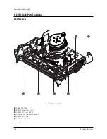
Exploded View and Parts List
Electric Parts List
Block Diagram
Schematic Diagrams
1.
2.
3.
4.
5.
6.
7.
8.
9.
Summary of Contents for CFTD2083TX/SMS
Page 2: ...ELECTRONICS Samsung Electronics Co Ltd JULY 2002 Printed in Korea AA82 00093A ...
Page 9: ...Samsung Electronics 3 1 2 Specifications ...
Page 10: ...MEMO 3 2 Samsung Electronics ...
Page 91: ...8 4 Samsung Electronics MEMO ...
Page 92: ...Schematic Diagrams 9 1 Samsung Electronics 9 1 MAIN 1 9 Schematic Diagrams ...
Page 93: ...Schematic Diagrams Samsung Electronics 9 2 9 2 MAIN 2 ...
Page 94: ...Schematic Diagrams Samsung Electronics 9 3 9 3 MAIN 3 ...
Page 95: ...Schematic Diagrams 9 4 Samsung Electronics 9 4 MAIN 4 ...
Page 96: ...Schematic Diagrams 9 5 Samsung Electronics 9 5 POWER BLOCK ...
Page 97: ...Schematic Diagrams 9 6 Samsung Electronics 9 6 DEFLECTION BLOCK ...
Page 98: ...Schematic Diagrams 9 7 Samsung Electronics 9 7 INTERFACE BLOCK ...
Page 99: ...Schematic Diagrams 9 8 Samsung Electronics 9 8 CRT BLOCK ...
Page 100: ...Schematic Diagrams 9 9 Samsung Electronics 9 9 Main Micom ...
Page 101: ...Schematic Diagrams 9 10 Samsung Electronics 9 10 AV Decoder ...