4-1, Meguro 1-chome, Meguro-ku, Tokyo 153-8654, Japan
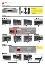
MULTI-CD/DAB CONTROL DSP HIGH POWER CD/MP3/WMA PLAYER WITH RDS TUNER
This service manual should be used together with the following manual(s):
CD Mech. Module:Circuit Description, Mech. Description, Disassembly
For details, refer to "Important symbols for good services".
Summary of Contents for Super Tuner III D DEH-P8600MP
Page 5: ...DEH P8600MP XN EW 5 5 6 7 8 5 6 7 8 C D F A B E 1 SPECIFICATIONS MC Service ...
Page 33: ...DEH P8600MP XN EW 33 5 6 7 8 5 6 7 8 C D F A B E ...
Page 36: ...DEH P8600MP XN EW 36 1 2 3 4 1 2 3 4 C D F A B E A A TUNER AMP UNIT IC Q TEST PCL MC Service ...
Page 37: ...DEH P8600MP XN EW 37 5 6 7 8 5 6 7 8 C D F A B E A SIDE B MC Service ...
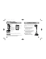
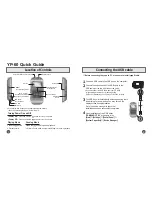
Page 79: ...DEH P8600MP XN EW 79 5 6 7 8 5 6 7 8 C D F A B E 8 OPERATIONS ...
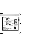
Page 80: ...DEH P8600MP XN EW 80 1 2 3 4 1 2 3 4 C D F A B E MC Service ...
Page 81: ...DEH P8600MP XN EW 81 5 6 7 8 5 6 7 8 C D F A B E ...
Page 83: ...DEH P8600MP XN EW 83 5 6 7 8 5 6 7 8 C D F A B E ...