ORDER NO.
PIONEER CORPORATION
4-1, Meguro 1-chome, Meguro-ku, Tokyo 153-8654, Japan
PIONEER ELECTRONICS SERVICE, INC. P.O. Box 1760, Long Beach, CA 90801-1760, U.S.A.
PIONEER ELECTRONIC (EUROPE) N.V. Haven 1087, Keetberglaan 1, 9120 Melsele, Belgium
PIONEER ELECTRONICS ASIACENTRE PTE. LTD. 253 Alexandra Road, #04-01, Singapore 159936
PIONEER CORPORATION 1999
c
ZY
‡
AC230V Adapter or Battery pack
ZU/CA
‡
AC120V Adapter or Battery pack
ZL
‡
AC230V Adapter or Battery pack
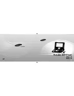
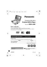
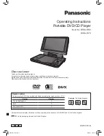
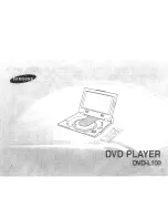
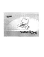
PDV-LC10
RRV2212
1. SAFETY INFORMATION ...................................... 2
2. EXPLODED VIEWS AND PARTS LIST ................ 4
3. BLOCK DIAGRAM AND SCHEMATIC DIAGRAM .. 12
4. PCB CONNECTION DIAGRAM .......................... 31
5. PCB PARTS LIST ............................................... 38
6. ADJUSTMENT .................................................... 42
CONTENTS
T – ZZR SEPT. 1999 Printed in Japan
THIS MANUAL IS APPLICABLE TO THE FOLLOWING MODEL(S) AND TYPE(S).
PORTABLE DVD PLAYER
Type
Power Requirement
Remarks
Model
PDV-LC10
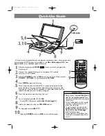
DIGITAL OUT (OPTICAL)
PHONES
HOLD
ON/OFF
COLOR
BRIGHT
MONITOR
7. GENERAL INFORMATION ................................ 44
7.1 DIAGNOSIS ................................................. 44
7.1.1 DISASSEMBLY ...................................... 44
7.1.2 TROUBLE SHOOTING .......................... 47
7.2 PARTS ......................................................... 48
7.2.1 IC ............................................................ 48
7.2.2 DISPLAY ..................................................... 61
8. PANEL FACILITIES AND SPECIFICATIONS .... 62