background image

ORDER NO.

PIONEER ELECTRONIC CORPORATION

4-1, Meguro 1-Chome, Meguro-ku, Tokyo 153-8654, Japan

PIONEER ELECTRONICS SERVICE, INC.  P.O. Box 1760, Long Beach, CA 90801-1760, U.S.A.
PIONEER ELECTRONIC (EUROPE) N.V .   Haven 1087, Keetberglaan 1, 9120 Melsele, Belgium
PIONEER ELECTRONICS ASIACENTRE  PTE. LTD.  501 Orchard Road, #10-00 Wheelock Place, Singapore 238880

PIONEER ELECTRONIC CORPORATION   1998

7. GENERAL INFORMATION .............................. 49

7.1 PARTS ....................................................... 49

7.1.1 IC ....................................................... 49
7.1.2 DISPLAY ........................................... 60

7.2 DIAGNOSIS ................................................ 61

7.2.1 DISASSEMBLY ................................. 61
7.2.2 DETAILS OF ERROR DISPLAY ....... 63

7.3 BLOCK DIAGRAM ...................................... 65

8. PANEL FACILITIES AND SPECIFICATIONS

....................................................... 66
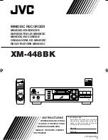
MINIDISC RECORDER

RRV1963

MJ-D707

MJ-17D

1. SAFETY INFORMATION .................................... 2
2. EXPLODED VIEWS AND PARTS LIST ............. 4
3. SCHEMATIC DIAGRAM ................................... 12
4. PCB CONNECTION DIAGRAM ....................... 28
5. PCB PARTS LIST ............................................. 37
6. ADJUSTMENT .................................................. 41

CONTENTS

T–DZE   JUNE  1998  Printed in Japan

KU

AC120V

MY

––

AC220–230V

MY/GR/FR

––

AC220–230V

THIS MANUAL IS APPLICABLE TO THE FOLLOWING MODEL(S) AND TYPE(S).

Model

MJ-D707

MJ-17D

Type

Power Requirement

Remarks

MINIDISC  RECORDER

MJ-D707

TIMER

REC

OFF

PLAY

DISC  LOADING  MECHANISM

PUSH ENTER

EDIT

/

NO

NAME

ANALOG

COAX

OPT

0

1

2

3

4

5

6

7

8

9

10

INPUT  SELECTOR

REC  LEVEL

DIGITAL

NR

REPEAT

A   B

TIME SKIP

PLAY
MODE

REC

MODE

NAME

CLIP

DISPLAY

/ CHARA

STANDBY

POWER

— 

OFF   

ON

SYNCHRO

REC

MIN

MAX

PHONES

LEVEL

)  

EJECT

$

$

!

!

#

*

&

Î

Legato  Link  Conversion

Summary of Contents for MJ-17D

Page 1: ...NEL FACILITIES AND SPECIFICATIONS 66 MINIDISC RECORDER RRV1963 MJ D707 MJ 17D 1 SAFETY INFORMATION 2 2 EXPLODED VIEWS AND PARTS LIST 4 3 SCHEMATIC DIAGRAM 12 4 PCB CONNECTION DIAGRAM 28 5 PCB PARTS LIST 37 6 ADJUSTMENT 41 CONTENTS T DZE JUNE 1998 Printed in Japan KU AC120V MY AC220 230V MY GR FR AC220 230V THIS MANUAL IS APPLICABLE TO THE FOLLOWING MODEL S AND TYPE S Model MJ D707 MJ 17D Type Powe...

Page 2: ...ch as Simpson Model 229 2 or equivalent between the earth ground and all exposed metal parts of the appliance input output terminals screwheads metal overlays control shaft etc Plug the AC line cord of the appliance directly into a 120V AC 60 Hz outlet and turn the AC power switch on Any current measured must not exceed 0 5 mA FOR USA MODEL ONLY Also test with plug reversed Using AC adapter plug a...

Page 3: ...ser pick up assembly provide the photo diodes and APC Auto Power Control circuit The photo diode detect output of the laser diode then IC104 control the APC circuit according to the signal voltage of the photo diode via IC101 The Variable resistancer on the FPC in the Laser pick up assembly can be adjusted the output level of Laser diode to fix the rated output level Laser Interlock Switch The loa...

Page 4: ... XY Z 3 8 11 MJ D707 KU MY only 10 7 6 9 5 4 1 1 2 2 1 2 2 2 2 1 2 2 12 MJ D707 MY MY GR FR only 13 MJ D707 MY only 14 MJ 17D KU only 2 EXPLODED VIEWS AND PARTS LIST NOTES Parts marked by NSP are generally unavailable because they are not in our Master Spare Parts List The mark found on some component parts indicates the importance of the safety factor of the part Therefore when replacing be sure ...

Page 5: ...2 CONTRAST TABLE 1 Protector F RHA1238 2 Protector R RHA1239 3 Packing Case See Contrast table 2 4 Sheet 750 600 0 5 Z23 007 5 Audio Cord L 1m PDE1248 6 Remote Control Unit RPX1131 CU MJ011 7 Battery Cover RZN1156 NSP 8 Batteries AA R6P VEM 013 9 Polyethylene Bag Z21 038 0 03 230 340 NSP 10 Warranty Card See Contrast table 2 11 Operating Instructions See Contrast table 2 12 Operating Instructions ...

Page 6: ... 25 28 25 24 29 21 17 11 15 37 12 33 33 1 5 21 10 9 14 21 31 30 21 9 10 21 16 21 23 MY and MY GR FR types only 23 22 36 CN402 CN403 CN601 CN602 CN401 Refer to 2 3 FRONT PANEL SECTION Refer to 2 4 MD MECHANISM ASSY 34 35 20 Except MJ 17D KU MJ 17D KU only MJ 17D KU only 20 Except MJ 17D KU 2 2 EXTERIOR ...

Page 7: ...RANS UNIT ASSY See Contrast table 2 3 Strain Relief See Contrast table 2 4 AC Power Cord See Contrast table 2 5 Lead Card 30P RDD1402 6 Fuse See Contrast table 2 7 Power Transformer RTT1316 NSP 8 PCB Holder PNW2100 9 Float Screw RBA1133 10 Float Rubber REB1328 11 Rear Panel See Contrast table 2 12 Mecha Angle RNB1133 13 Under Base RNB1134 14 Shield Case RNB1139 NSP 15 PC Support VEC1549 NSP 16 MD ...

Page 8: ...MJ D707 MJ 17D 8 2 3 FRONT PANEL SECTION A A 1 2 14 15 21 9 17 7 19 13 10 20 18 23 23 12 1 2 12 2 2 11 16 22 3 8 12 1 2 12 2 2 Cut Cut Cut Not used 23 6 5 4 24 ...

Page 9: ...ton B RAC2216 17 Front Panel See Contrast table 2 18 Door See Contrast table 2 19 Display Window RAH2862 20 FL Sheet See Contrast table 2 21 Panel Stay B RNT1250 22 Screw ABA7009 23 Screw PPZ30P100FMC 24 Edge Guard RBK1078 1 DISPLAY UNIT ASSY RWZ4310 RWZ4294 RWZ4294 RWZ4289 2 CONTROL UNIT ASSY RWZ4311 RWZ4295 RWZ4295 RWZ4290 3 HEADPHONE UNIT ASSY RWZ4312 RWZ4296 RWZ4296 RWZ4291 17 Front Panel RAH2...

Page 10: ...8 43 40 33 44 31 28 32 34 40 11 5 10 17 7 6 4 9 37 19 21 20 18 37 16 26 15 13 14 37 12 53 52 51 A E E F F G G H A B B C C D D 37 8 40 24 25 39 27 41 35 36 29 39 46 23 30 45 2 3 50 47 37 CN103 CN101 CN102 CN105 1 H 2 4 MD MECHANISM ASSY ...

Page 11: ...2 Screw RBA1129 23 Spindle Spring RBH1460 24 Lifter SP RBH1462 25 Screw Guide RBK1072 26 S H Spring RBK1073 27 Guide Shaft RLA1310 28 Lead Screw RLA1311 29 Shield Case RNE1950 30 Reference Plate RNK2306 31 S Holder RNK2307 32 Worm Wheel RNK2309 33 Hook RNK2310 34 Head Lifter RNK2311 35 MD Head RPB1062 36 MD Pick up RWY1018 37 Screw IPZ20P080FMC 38 Screw JFZ17P020FZK 39 Screw JGZ14P020FMC 40 Screw ...

Page 12: ...4311 MJ D707 MY RWZ4295 MJ D707 MY GR FR RWZ4295 MJ 17D KU RWZ4290 CONTROL UNIT ASSY F CORE MAIN UNIT ASSY RWZ4271 MD MECHANISM ASSY RXA1773 A CORE SW UNIT ASSY RWZ4272 B PARALLEL JUMPER PARALLEL JUMPER LEAD CARD LEAD CARD To LOADING MOTOR To SPINDLE MOTOR To SLED MOTOR To REC HEAD To PICKUP ORANGE BLUE BLACK RED AC POWER CORD KU type PDG1015 AC120V 60Hz MY MY GR FR type PDG1003 AC220 230V 50 60Hz...

Page 13: ...KU RWZ4309 MJ D707 MY RWZ4293 MJ D707 MY GR FR RWZ4293 MJ 17D KU RWZ4288 MAIN UNIT ASSY C MJ D707 KU RWZ4312 MJ D707 MY RWZ4296 MJ D707 MY GR FR RWZ4296 MJ 17D KU RWZ4291 HEADPHONE UNIT ASSY G MJ D707 KU RWZ4310 MJ D707 MY RWZ4294 MJ D707 MY GR FR RWZ4294 MJ 17D KU RWZ4289 DISPLAY UNIT ASSY E PARALLEL JUMPER PARALLEL JUMPER PARALLEL JUMPER C 1 2 C 2 2 ...

Page 14: ... CORE MAIN UNIT and CORE SW UNIT ASSEMBLIES B A CORE MAIN UNIT ASSY RWZ4271 A CORE SW UNIT ASSY RWZ4272 B LOADING MOTOR SLED MOTOR SPINDLE MOTOR YELLOW BLACK ORANGE BLUE BLACK RED INSIDE SW A DISC PROTECT B DISC MEDIA DETECT PICKUP 1 2 3 10 11 8 9 ...

Page 15: ...15 A B C D 5 6 7 8 5 6 7 8 A INSIDE C CN401 YB 0 01 R291 R293 47k PLAYBACK SIGNAL REC SIGNAL OUTPUT DIGITAL AUDIO SIGNAL INPUT DIGITAL AUDIO SIGNAL RF SIGNAL SIGNAL ROUTE 6 5 7 4 1 are waveform Nos on pages 26 and 27 ...

Page 16: ... 0V 3 18V 0 02V 3 19V 3 2V 0V 0 05V 3 18V 3 19V 0 51V 0 4V 0 3V 0 55V 9 8 7 6 5 4 3 2 1 30 29 28 27 26 25 24 23 22 21 20 19 18 17 16 15 14 13 12 11 10 49 48 47 46 45 44 43 42 41 40 39 38 37 36 35 34 33 32 31 PIN NO VOLTAGE 50 IC104 0 54V 0 6V 0 6V 0 6V 0V 0V 0V 0V 3 2V 0V 0V 3 2V 0V 0V 3 2V 0V 0V 0V 0V 0V 0V 3 1V 3 2V 0V 0V 3 2V 0V 0V 0V 3 2V 0V 3 19V 0V 3 19V 0V 3 18V 3 2V 0V 1 03V 1 6V 0 56V 1 4...

Page 17: ... 99V 4 99V 1 61V 1 62V 2 46V 2 51V 0V 0V 2 54V 2 45V 1 62V 1 62V 1 61V 3 17V 0V 1 61V 1 61V 1 61V 1 61V 1 36V 1 36V 1 61V 1 61V 1 63V 2 41V 2 55V 2 47V 2 48V 0V 0V 2 79V 2 18V 0V 1 69V 5 0V 4 99V 1 67V 1 69V 1 69V 9 8 7 6 5 4 3 2 1 30 29 28 27 26 25 24 23 22 21 20 19 18 17 16 15 14 13 12 11 10 42 41 40 39 38 37 36 35 34 33 32 31 VOLTAGE IC106 PIN NO 1 66V 1 62V 1 62V 0V 1 67V 1 67V 1 67V 3 19V 8 7...

Page 18: ...MY MY GR FR type PDG1003 AC220 230V 50 60Hz FU1 FUSE KU type REK1075 1A 125V MY MY GR FR type REK1019 500mA 250V JUMPER KU type W305 MY MY GR FR type W306 C203 C205 C207 C214 CFTLA 0 1 JA601 RKB1032 D303 D306 S5566G TPB2 C315 C319 MJ D707 KU CEAT470M16 other models PCH1123 C503 C504 MJ D707 KU CEAT470M16 other models CEBA220M25 C50 MJ D othe C313 C314 MJ D707 KU CEAT other models PCH1120 C313 PCH1...

Page 19: ...M16 other models RCH1133 120 C313 121 C314 IC603 NJM4580D CAUTION FOR CONTINUED PROTECTION AGAINST RISK OF FIRE REPLACE ONLY WITH SAME TYPE NO 491 400 MFD BY LITTELFUSE INK FOR IC301 IC303 IC305 AEK7004 CAUTION FOR CONTINUED PROTECTION AGAINST RISK OF FIRE REPLACE ONLY WITH SAME TYPE NO 49103 5 MFD BY LITTELFUSE INK FOR IC201 AEK7017 MY GR FR y 2 2 50 2 2 50 470k 470k 100 1 4W 100 1 4W 68k 68k 18 ...

Page 20: ...3 4 1 2 3 4 3 4 MAIN UNIT ASSY 2 2 E J702 E J703 DSP built in 20 bit ADC DAC C604 C612 C616 MJ D707 KU CEAT470M16 other models VCH1081 C614 MJ D707 KU CEAT221M6R3 other models VCH1081 L306 RTF MY and M types only 12 16 14 15 13 17 C ...

Page 21: ... RWZ4288 MAIN UNIT ASSY 2 2 RKB1021 R455 MY MY GR FR types only KU type only L406 RTF1167 L307 RTF1167 MY and MY GR FR types only MY and MY GR FR types only L306 RTF1167 MY and MY GR FR types only PLAYBACK SIGNAL REC SIGNAL OUTPUT DIGITAL AUDIO SIGNAL INPUT DIGITAL AUDIO SIGNAL SIGNAL ROUTE C are waveform Nos on pages 26 and 27 ...

Page 22: ...MJ D707 MJ 17D 22 A B C D 1 2 3 4 1 2 3 4 CN402 CN403 MD µ COM MD µ COM MD µ COM CHASSIS SYSTEM CONTROLER PDG222B C C 3 5 DISPLAY UNIT CONTROL UNIT and HEADPHONE UNIT ASSEMBLIES ...

Page 23: ...904 CCSQCH 100P RDF1155 1 2 BLACK CHASSIS DISPLAY UNIT ASSY S701 JOG DIAL S702 FAST REVERSE S703 NAME S704 EDIT NO S705 FAST FORWARD S706 SYNCHRO REC S707 RECORD S708 STOP S709 MD EJECT S710 PAUSE S711 PLAY S712 INPUT SELECTOR CONTROL UNIT ASSY S801 TIMER S802 DISPLAY CHARA S803 NAME CLIP S804 DIGITAL NR S805 REC MODE S806 TIME SKIP S807 A B S808 REPEAT S809 PLAY MODE MJ D707 KU RWZ4312 MJ D707 MY...

Page 24: ...13V 9 31V 0 013V 0 013V 0 027V 8 49V 8 7 6 5 4 3 2 1 PIN NO VOLTAGE IC603 0V 0V 0V 0V 0V 0V 5 0V 5 0V 0V 0V 0V 5 0V 0V 0V 0V 0V 0V 0V 0V 0V 0V 2 5V 2 5V 0V 5 0V 0V 0V 2 3V 2 6V 5 0V 0 15V 4 9V 0V 5 0V 4 9V 0 18V 4 8V 4 8V 0 15V 1 7V 0 3V 3 3V 2 5V 2 5V 3 3V 2 5V 2 5V 2 5V 2 5V 2 5V 9 8 7 6 5 4 3 2 1 30 29 28 27 26 25 24 23 22 21 20 19 18 17 16 15 14 13 12 11 10 49 48 47 46 45 44 43 42 41 40 39 38 ...

Page 25: ...1 10 49 48 47 46 45 44 43 42 41 40 39 38 37 36 35 34 33 32 31 PIN NO VOLTAGE 50 IC701 23 3V 11 9V 14 2V 18 9V 16 6V 14 5V 23 5V 21 1V 23 3V 12 3V 14 4V 23 5V 18 8V 18 8V 12 2V 14 4V 14 3V 12 1V 16 6V 16 7V 12 1V 16 4V 16 5V 18 8V 12 1V 14 4V 23 5V 19 1V 21 2V 14 4V 18 9V 18 9V 16 6V 16 7V 16 7V 29 5V 28 0V 28 0V 5 0V 28 0V 28 0V 28 0V 28 0V 28 0V 28 0V 28 0V 28 0V 28 0V 28 0V 28 0V 59 58 57 56 55 ...

Page 26: ... UNIT ASSY MODE STOP GND DC1V div 1mSec div 6 GND DC500mV div 2mSec div IC102 pin77 TE MON CORE MAIN UNIT ASSY MODE PLAY DISC TGTS1 or MMD 110 7 IC102 pin54 TES01 CORE MAIN UNIT ASSY MODE STOP GND DC2V div 10 µSec div 4 GND DC1V div 0 2 µSec div IC102 pin50 EFMO CORE MAIN UNIT ASSY MODE REC DISC GGF1328 MMD 212 5 IC102 pin75 FE MON CORE MAIN UNIT ASSY MODE PLAY DISC TGTS1 or MMD 110 GND DC100mV di...

Page 27: ... 212 GND DC2V div 0 5 µSec div 14 GND DC2V div 0 5 µSec div CN602 pin20 DA DATA MAIN UNIT ASSY MODE PLAY 1 kHz 0 dB 15 IC602 pin23 LRCK MAIN UNIT ASSY MODE PLAY 1 kHz 0 dB GND DC2V div 10 µSec div 17 GND DC2V div 0 2mSec div CN602 pin85 LOUT MAIN UNIT ASSY MODE PLAY 1 kHz 0 dB 18 IC603 pin1 MAIN UNIT ASSY MODE PLAY 1 kHz 0 dB GND AC2V div 0 2mSec div 16 IC602 pin22 BCLK MAIN UNIT ASSY MODE PLAY 1 ...

Page 28: ...ral destinations For further information for respective destinations be sure to check with the schematic diagram 4 View point of PCB diagrams Symbol In PCB Diagrams Symbol In Schematic Diagrams Part Name B C E D D G G S S B C E B C E D G S B C E B C E B C E Transistor Transistor with resistor Field effect transistor Resistor array 3 terminal regulator Capacitor Connector P C Board Chip Part SIDE A...

Page 29: ...OTOR REC HEAD PICKUP ASSY IC101 IC112 IC108 IC113 IC113 IC109 IC110 IC116 Q103 Q104 IC106 IC102 IC103 IC104 IC114 Q101 Q102 RNP1721 B RNP1721 B CORE MAIN UNIT ASSY A 1 2 6 7 5 9 8 4 10 11 3 SIDE B SIDE A 4 2 CORE MAIN UNIT ASSEMBLY 1 are waveform Nos on pages 26 and 27 ...

Page 30: ...MJ D707 MJ 17D 30 A B C D 1 2 3 4 1 2 3 4 A CN104 NEUTRAL LIVE AC POWER CORD TRANS UNIT ASSY D MAIN UNIT ASSY C IC201 IC305 IC301 IC303 RNP1726 C H J10 4 3 MAIN UNIT and TRANS UNIT ASSEMBLIES SIDE A ...

Page 31: ...MJ D707 MJ 17D 31 A B C D 5 6 7 8 5 6 7 8 04 E J102 E J102 E J103 G J901 03 IC405 IC307 RNP1726 C H J1001 12 15 16 13 14 18 17 SIDE A are waveform Nos on page 25 ...

Page 32: ...MJ D707 MJ 17D 32 A B C D 1 2 3 4 1 2 3 4 IC604 Q504 Q502 IC605 Q604 Q601 Q603 Q605 Q303 Q602 IC401 IC402 Q503 IC602 IC407 IC406 IC404 IC403 Q501 MAIN UNIT ASSY C RNP1726 C SIDE B ...

Page 33: ...MJ D707 MJ 17D 33 A B C D 5 6 7 8 5 6 7 8 Q304 TRANS UNIT ASSY D RNP1726 C SIDE B ...

Page 34: ...MJ D707 MJ 17D 34 A B C D 1 2 3 4 1 2 3 4 4 4 DISPLAY UNIT and CONTROL UNIT ASSEMBLIES DISPLAY UNIT ASSY E CONTROL UNIT ASSY F RNP1726 C RNP1726 C SIDE A SIDE B SIDE A ...

Page 35: ...MJ D707 MJ 17D 35 A B C D 5 6 7 8 5 6 7 8 C CN402 C CN403 C CN601 CONTROL UNIT ASSY F DISPLAY UNIT ASSY E RNP1726 C RNP1726 C SIDE B SIDE B SIDE A ...

Page 36: ...MJ D707 MJ 17D 36 A B C D 1 2 3 4 1 2 3 4 4 5 HEADPHONE UNIT ASSEMBLY C CN602 HEADPHONE UNIT ASSY G RNP1726 C SIDE A SIDE B ...

Page 37: ...effective digits any digit apart from 0 such as 560 ohm and 47k ohm tolerance is shown by J 5 and K 10 560 Ω 56 101 561 RD1 4PU 5 6 1 J 47k Ω 47 10 3 473 RD1 4PU 4 7 3 J 0 5 Ω R50 RN2H Â 5 0 K 1 Ω 1R0 RS1P 1 Â 0 K Ex 2 When there are 3 effective digits such as in high precision metal film resistors 5 62k Ω 562 10 1 5621 RN1 4PC 5 6 2 1 F LIST OF WHOLE PCB ASSEMBLIES KU MY MY GR FR KU Part No Mark ...

Page 38: ...ot used 1SS133X L304 L307 L406 Not used RTF1167 Not used C313 CEAT332M16 PCH1120 PCH1120 3300µF 16V 3300µF 16V C314 CEAT222M16 PCH1121 PCH1121 2200µF 16V 2200µF 16V C315 C319 CEAT470M16 PCH1123 PCH1123 470µF 6 3V 470µF 6 3V C419 CKSQYF104Z25 Not used CKSQYF104Z25 C503 C504 CEAT470M16 CEBA220M25 CEBA220M25 C505 C508 C601 CEAT470M16 RCH1133 RCH1133 100µF 10V 100µF 10V C551 C552 CEAT2R2M50 CEBA2R2M50...

Page 39: ...602 AK7712A VQ IC306 BA05T IC604 M5218AFP IC601 NJM2100D IC406 NJM4558MD IC603 NJM4580D IC302 NJM7805FA IC307 S 806D IC605 SRM2B256SLMX70 IC404 TC74HC153AF IC401 IC402 TC74HCT08AF IC403 TC74HCU04AF IC407 TC9246F Q303 2SA1037K Q304 2SC2412K Q501 Q504 2SD2114K Q601 Q602 DTA124EK Q603 Q605 DTC124EK D307 1SR139 400 TA D308 D402 D602 1SS133X D401 D603 DAP202K D303 D306 S5566G TPB2 COILS AND FILTERS L40...

Page 40: ...R559 R560 RN1 10SE1202D Other Resistors RS1 10S J OTHERS CN602 3P JUMPER CONNECTOR 52147 0310 CN402 CN403 52147 1410 14P JUMPER CONNECTOR HEAT SINK ANH 575 CN601 KR CONNECTOR B6B PH K S JA401 OPTICAL LINK IN GP1F32R JA404 OPTICAL LINK OUT GP1F32T CN301 11P JUMPER CONNECTOR KPD11 JA403 1P JACK RKB1021 JA601 4P JACK with SHIELD PLATE RKB1032 JA405 JA406 JACK RKN1004 PCB BINDER VEF1040 CN401 30P CONN...

Page 41: ... 110 Commercial discs JIGS AND MEASURING INSTRUMENTS Adjustment points When Exchange Exchange Exchange Exchange Exchange Exchange Exchange PICKUP Servo Base Assy SPINDLE MOTOR CORE MAIN UNIT ASSY MD HEAD Loading Mechanism Assy Servo Mechanism Assy MD Mechanism Assy Loading Mechanism Assy Servo Mechanism Assy 3 4 Page 44 45 3 4 Page 44 45 4 Page 44 45 3 4 Page 44 45 3 4 Page 44 45 6 1 NECESSARY ADJ...

Page 42: ...k How to enter into test mode 1 1 Hold the ENTER key and the STOP key depressed and press the POWER switch 2 SYSTEM TEST will be displayed on the FL display Operation check for the operation keys Operation check for other keys Operation Keys FL Display OFF S Y S T E M T E S T TIMER SW REC Entire FL lit PLAY Entire FL not lit A B A B REPEAT R E P E A T PLAY MODE P L A Y M O D E TIME SKIP T I M E S ...

Page 43: ...est mode Laser Wavelength PLAY key depressed 780 nm 2 Press the NAME key ppw PLAY power output status 3 Measure the laser power with an optical power meter ppw 4 At this time check that the measuring value PLAY ppw May be omitted power meets the standard value of the table on the right Note When the standard value on the right is applied the numerical value immediately after entry into test mode 2...

Page 44: ...on diagram and loosen the screw A at the side of the adjustment hole Turn the hole with a screwdriver until the Lissajous waveform becomes as shown in the figure and then tighten the screw A 5 Press the STOP key Adjustment end 3 Grating Adjustment Connection Diagram Adjustment Point Step No Operation Keys and Operation Method FL Display Status Remarks 1 Power ON while holding the ENTER key and the...

Page 45: ...or at of000c0015 the time of focus offset 0 is displayed 5 Check the jitter value and end the adjustment when the intermediate jitter value is 29 nsec or less 6 Press the NAME CLIP key of 04 c0032 The C1 error with application of a focus offset of about 0 4 µm on the side is displayed The jitter value J at this time is recorded 5 Normal adjustment 6 Defocus adjustment Step No Operation Keys and Op...

Page 46: ...stment Connection diagram Jitter Meter LEVEL JITTER GND CORE MAIN UNIT ASSY SIDE A REFO EFM MON Step No Operation Keys and Operation Method FL Display Status Remarks 1 Power ON while holding the ENTER key and the EJECT Test mode PLAY key depressed 2 Insert the test disc GGF1328 MMD 212 LOADING GRT AJST 3 Perform Normal Adjustment step 3 step 4 AUTO AJST 4 Press the NAME CLIP key TEST PLAY TEST PLA...

Page 47: ...Perform steps 6 to 9 in this condition TEST PLAY 14 Press the EJECT key eject the test disc EJECT GGF1328 MMD 212 and insert TGYS1 or LOADING MMD 110 GRT AJST 15 Perform steps 3 to 13 and check the jitter C1 a0062 c0009 Check that the jitter value meets the standard error with the test disc TGYS1 or MMD 110 a03d2 c0007 value of the following table a0712 c0006 16 Press the EJECT key EJECT The test ...

Page 48: ...Y mode 14 Perform steps 5 to 13 of Jitter C1 Error Check a0069 c0009 Check the jitter C2 error at the inner at the time of Playback a03D9 c0007 intermediate outer circumference of GGF1277 At the time of self recording wait for seven a0719 c0006 and check that the jitter value satisfies the addresses after TEST PLAY start and then press standard value of the following table the REC key and enter in...

Page 49: ...p Input Output Control Circuit Address Buffer Line Decoder Column Decoder Output Buffer Input Buffer A0 A1 A2 A3 A4 A5 A6 A7 A8 9 24 DQ2 DQ3 25 DQ4 13 Vcc 3 3V 26 Vss 0V 22 2 DQ1 1 A9 5 CAS RAS W OE 7 GENERAL INFORMATION 7 1 1 IC 7 1 PARTS Block Diagram Pin Function M5M4V4400CTP 7 IC103 CORE MAIN UNIT ASSY DRAM Pin Assignment Top view The information shown in the list is basic information and may ...

Page 50: ...reversed output terminal 9 VM1 CH1 nonreversed output terminal 10 GND Motor GND 11 12 VM2 CH2 nonreversed output terminal 13 VM2 CH2 reversed output terminal 14 OUT2 E2 amplifier output terminal 15 IN2 E2 amplifier reversed input terminal 16 IN2 E2 amplifier nonreversed input terminal 17 MUTE1 Mute terminal CH1 to CH4 18 MUTE2 Mute terminal CH5 19 SS GND Small signal ground 20 VREF Reference volta...

Page 51: ...10 channels possible System clock generation XIN XOUT XCIN XCOUT UART clock synchronized SI O 8bits 2 channels SB R0H R0L R1H R1L R2 R3 A0 A1 FB INTB ISP USP ROM MEMORY 16 bits CPU CORE I O PORT RAM 10k bite Port P0 8 Port P1 8 Port P2 8 Port P3 8 Port P4 8 Port P5 8 Port P6 8 Port P7 8 Port P8 7 Port P85 Port P9 8 Port P10 8 Internal Peripheral Functions Monitoring timer 16 bits Register Stack Po...

Page 52: ...are the I O terminals of the main clock oscillation circuit Connect a ceramic oscillator or a crystal oscillator between the terminals XIN and XOUT In case of an externally generated clock enter the clock from the XIN terminal and leave the XOUT terminal open Impress 0 V Impress 2 7 V to 5 5 V These are 8 bit I O ports with the same functions as P0 By software selection they function as the I O te...

Page 53: ...of separate bus setting These are CMOS 8 bit I O ports They have direction registers for I O selection and input or output port setting is possible individually for each terminal For an input port the existence or absence of a pull up resistance can be set by software in 4 bit units Data D0 to D7 I O is performed at the time of separate bus setting This are 8 bit I O ports with the same functions ...

Page 54: ...error signal A 6 EIN I Tracking error signal E 7 TCG I Track cross signal 8 BIN I Focus error signal B 9 FIN I Tracking error signal F 10 VBAT I Power supply voltage detection signal for constant voltage servo 11 WBI I ADIP wobble signal 12 VDD1 Digital power supply 13 DGND Digital GND 14 TEST0 I Test use input normally connected to GND when used 15 TEST1 I 16 TEST2 I Test useinput Encoder ServoMo...

Page 55: ... VPO O PLL phase error input for varying pitch 62 VDD1 Digital power supply 63 DGND Digital GND 64 XI I Oscillation circuit input 33 8688MHz 65 XO O No Name I O Description 66 DIN I Digital input signal 67 DOUT O Digital output signal 68 VDD3 Power supply for internal PLL 69 DGND Digital GND 70 LRCK O Music data Lch Rch changeover output 71 BCLK O Music data shift lock 72 DFCK O Clock for AD DA co...

Page 56: ...MJ D707 MJ 17D 56 PDG222B IC701 DISPLAY UNIT ASSY System Control µ com Block Diagram Pin Assignment Top view ...

Page 57: ... PB5 SCK1 IO IO Serial clock CH1 Input Output terminal 26 PB6 SC1 IO I Serial data CH1 input terminal 27 PB7 SO1 IO O Serial data CH1 output terminal 28 AVREF A Dconverterreferencevoltageinputterminal 29 PA0 AN0 I O A D converter analog input terminal 36 PA7 AN7 37 AVss A D converter GND terminal 38 RST System reset terminal L Active 39 EXTAL I System clock oscillation crystal connection terminal ...

Page 58: ... RegDRV External PNP drive output for the regulator 19 RegOUT Regulator output emitter follower output 20 RegNF Regulator feedback terminal Pre Driver 20 19 18 17 16 15 14 13 12 11 1 2 3 4 5 6 7 8 9 10 Vreg IN Reg NF Reg OUT Reg DRV VOS2 VDD VOS1 VOD1 VOD2 N C VSS Reg GND Reg SEL VG SVCC PD GND EFM MUTE N C N C No Name Description 1 VregIN Regulator input and regulator power supply 2 RegGND Regula...

Page 59: ...gnal inversion signal 17 XSGAIN Logic signal output terminal outputs SGAIN signal inversion signal 18 AGND Analog part GND terminal 19 DGND Digital part GND terminal 20 DTEMP Tip temperature detection terminal 21 LATCH Latch signal input terminal 22 CLOCK Clock signal input terminal 23 DATA Serial data input terminal 24 DVCC Digital part power terminal 25 FOUT Servo use signal amp Tracking servo s...

Page 60: ...2 13 14 15 17 18 19 20 21 22 23 24 25 16 1 2 3 4 5 6 TOC DNR D VOL COAXIAL OPTICAL ANALOG REMAIN TOTAL REHEARSAL 1 SYNCHRO S CUT A MARK MONO ALCA ADLC REC DISC TRACK TIME DATE L R B3 B4 B5 B6 B7 B8 B9 B10 B11 B12 B13 B14 B15 B16 B17 B18 B19 B20 B21 B22 B23 B24 B25 B26 B27 B28 B29 B30 B31 B32 P36 S1 P35 5 7 P34 4 7 S2 P33 3 7 P32 2 7 B32 P31 1 7 B31 P30 5 6 B30 P29 4 6 B29 P28 3 6 B28 P27 2 6 B27 2...

Page 61: ... CORE MAIN UNIT ASSY 4 After the Carrier has been pushed in move the Upper Slider to the rear and stop it at the position where the Under Slider starts to move 5 Shift part B to the position shown in the figure while raising the Under Slider At the same time the Upper Slider moves to the front 6 Remove the Lock Plate One screw B 7 Remove the Servo Mechanism Assy Caution for the time of installatio...

Page 62: ...g One screw C 4 Remove the hook of the S H Spring as shown in the figure on the right 5 Remove the Safety Screw 6 Raise the left side of the Guide Shaft and pull it out to the left 7 Remove the MD Pick up With the front facing down remove it to the front At this time the MD Pick up can be removed more easily when the Reference Plate is removed Removal of the MD Pick up MD Pick up Installation Perf...

Page 63: ...ring music number and character information during REC PLAY music name disc number etc FTNO LTNO FTNO 0 or 1 UTOC recorded on DISC could not be read Start address End address Any one data of UTOC 0 to 4 has looped Measure Check if there are scratches dusts fingerprints or black spots on disc Check if disc fluctuates eccentrically or moves up and down largely Check if CD is copy proof Example CD R ...

Page 64: ... 0 Focus execution error etc occurred due to shock during REC PLAY UTOC read was correct but could not be rewrite it The EEPROM data are incorrect Never completes EJECT Never moves HEAD UP Never moves HEAD DOWN The set microcomputer and MD mechanism microcomputer are not communicating properly Measure Select other TNO or replace with other discs Disc is outside specifications Replace with differen...

Page 65: ...LR376481 S RAM IC605 SRM2B256SLMX70 A D D A in D S P IC602 AK7712A VQ SYSTEM C P U IC701 PDG222B HEADPHONE AMP IC604 M5218AFP L P F IC603 INPUT AMP IC601 NJM2100D INPUT VOLUME VR701 INPUT SELECTOR IC604 TC74HC153AF DUTY CORRECTER IC403 IC406 MECHA C P U IC104 PD5450A DRIVER IC106 M56758FP BUFFER 3V 5V CONVERTER IC401 IC402 OPTICAL DIGITAL OUT DIGITAL IN OPTICAL LINE IN LINE OUT HEADPHONE JACK COAX...

Page 66: ...lay 3 button s Fast forward button d Fast reverse 1 button f Remote control sensor g DISPLAY CHARA button h NAME CLIP button j REC MODE button k PLAY MODE button LINE INPUT OUTPUT REC PLAY COAXIAL OPTICAL DIGITAL INPUT DIGITAL OUTPUT OPTICAL L R CONTROL IN OUT Main unit rear panel To connect to equipment with the Pioneer Î mark U S model only Use a commercialy available miniplug cord without load ...

Page 67: ...gital input recording of an optical in put f Indicates analog input recording g Indicates that the digital volume control function is active h Indicates that the digital NR function is active j Indicates that recording or editing has been per formed k Indicates that time information is selected as shown in the display section l Indicates that the track data as shown in the dis play has been select...

Page 68: ...bject to possible modification with out notice due to improvements MAINTENANCE OF EXTERNAL SURFACES Use a polishing cloth or dry cloth to wipe off dust and dirt When the surfaces are very dirty wipe with a soft cloth dipped in some neutral cleanser diluted five or six times with water and wrung out well and then wipe again with a dry cloth Do not use furniture wax or cleaners Never use thinners be...

Reviews: