background image

6-DISC MULTI-MINI DISC PLAYER

MD-P100 

EW

S

ervice

M

anua

l

PIONEER ELECTRONIC CORPORATION

4-1, Meguro 1-Chome, Meguro-ku, Tokyo 153-8654, Japan 

PIONEER ELECTRONICS SERVICE INC.     

P.O.Box 1760, Long Beach, CA 90801-1760 U.S.A.

PIONEER ELECTRONIC [EUROPE] N.V.    

Haven 1087 Keetberglaan 1, 9120 Melsele, Belgium 

PIONEER ELECTRONICS ASIACENTRE PTE.LTD.   

501 Orchard Road, #10-00, Lane Wheelock Place, Singapore 23880

PIONEER ELECTRONIC CORPORATION 1998 

ORDER NO.

CRT2203

CONTENTS

1. SAFETY INFORMATION ............................................2

2. EXPLODED VIEWS AND PARTS LIST .......................2

3. SCHEMATIC DIAGRAM .............................................8

4. PCB CONNECTION DIAGRAM ................................18

5. ELECTRICAL PARTS LIST ........................................26

6. ADJUSTMENT..........................................................29

7. GENERAL INFORMATION .......................................30

7.1 IC .........................................................................30

7.2 DISASSEMBLY ...................................................40

7.3 BLOCK DIAGRAM ..............................................44

8. OPERATIONS AND SPECIFICATIONS.....................46

-

US and foreign patents licensed from Dolby Laboratories Licensing Corporation.

K-FEA. APR. 1998 Printed in Japan

Summary of Contents for MD-P100

Page 1: ...ASIACENTRE PTE LTD 501 Orchard Road 10 00 Lane Wheelock Place Singapore 23880 C PIONEER ELECTRONIC CORPORATION 1998 ORDER NO CRT2203 CONTENTS 1 SAFETY INFORMATION 2 2 EXPLODED VIEWS AND PARTS LIST 2 3 SCHEMATIC DIAGRAM 8 4 PCB CONNECTION DIAGRAM 18 5 ELECTRICAL PARTS LIST 26 6 ADJUSTMENT 29 7 GENERAL INFORMATION 30 7 1 IC 30 7 2 DISASSEMBLY 40 7 3 BLOCK DIAGRAM 44 8 OPERATIONS AND SPECIFICATIONS 4...

Page 2: ... affixed to the rear of the player CLASS 1 LASER PRODUCT PACKING SECTION PARTS LIST Mark No Description Part No Part No PIONEER SONY Mark No Description Part No Part No PIONEER SONY NOTE Parts marked by are generally unavailable because they are not in our Master Spare Parts List Screws adjacent to mark on the product are used for disassembly 1 Cord CZD3030 177777311 2 Cord CZD3036 177777421 3 Bas...

Page 3: ...amper CZN5071 393017601 13 Spring CZB3038 393017701 14 Case Lower CZN5142 393017391 15 Cushion CZN5085 393169701 16 Cushion CZN5068 334875003 17 Cord CZD3037 177777221 18 Self Tapping Screw CZB3041 768510411 19 Self Tapping Screw CZB3042 768513311 20 PTT CZB3039 762177560 21 BVTT CZB3037 391295611 22 Sheet CZN5080 393374001 23 Cushion CZN5079 383144111 24 Spacer CZN5117 393074401 25 Cushion CZN506...

Page 4: ...crew CZB3036 390941201 5 Sensor PCB CZN5087 165888413 6 Cushion CZN5068 334875003 7 Cushion CZN5069 371597301 8 Cushion CZN5075 393169901 9 Sheet CZN5072 393102503 10 Cushion CZN5074 393169801 11 PCB CZN3100 166294211 12 Screw CZB3073 302397401 MAIN PCB SECTION PARTS LIST Mark No Description Part No Part No PIONEER SONY Mark No Description Part No Part No PIONEER SONY ...

Page 5: ...01 14 Chassis Bottom A Assy CZX3065 X33755301 15 Gear CZN5097 393031301 16 Gear ELV2 CZN5145 302038601 17 Worm Wheel ELV2 CZN5147 302036301 18 Switch CZS3038 157077111 19 Switch CZS3039 157077121 20 Screw CZB3048 762785237 21 Screw CZB3049 762755407 22 Screw CZB3059 762785507 23 LD Motor Assy CZX3076 X33715082 24 ELV Motor Assy CZX3077 X33748121 2 3 4 1 1 5 6 7 24 not supplied 8 17 9 10 11 9 9 12 ...

Page 6: ...5002 12 Holder Caddie Assy CZX3026 X33712165 13 Spring D Lock CZB3064 393035202 14 Loading Slider 2 Assy CZX3070 X33746722 15 Rack Loading CZN5115 393036601 16 Spring CZB3068 393036001 17 Chassis Rear 2 Assy CZX3064 X33746712 18 Spring Lock CZB3062 393034901 19 Plate Holder Assy CZX3027 X33712195 20 Washer CZN5111 302151101 21 Screw CZB3048 762785237 MD 2 SECTION PARTS LIST Mark No Description Par...

Page 7: ...08 393034202 15 Holder SLB CZN5104 393033601 16 Spring CZB3052 393033501 17 Holder CZX3022 X33712131 18 Screw CZX3023 X33712141 19 Guide OPA CZL3002 393033101 20 Spring CZN5105 393033701 21 Mini Disc Device CZG3005 858303501 22 Servo PCB Assy CZW3054 A3222980A 23 Screw CZB3054 393275501 24 SP Motor CZX3019 A3291507A 25 SL Motor Assy CZX3020 A3291508A 26 Slide Variable Resistor CZC5118 122381712 27...

Page 8: ...8 MD P100 1 2 3 4 1 2 3 4 D C B A 3 SCHEMATIC DIAGRAM 3 1 SERVO PCB ASSY A SERVO PCB ASSY A MINI DISC DEVICE ...

Page 9: ...9 MD P100 5 6 7 8 5 6 7 8 D C B A Note When ordering service parts be sure to refer to EXPLODED VIEWS AND PARTS LIST or ELECTRICAL PARTS LIST A B CN500 ...

Page 10: ... Waveforms 10 MD P100 ...

Page 11: ...3 2 MAIN PCB Waveforms 11 MD P100 ...

Page 12: ...12 MD P100 1 2 3 4 1 2 3 4 D C B A CN200 A MAIN PCB B B ...

Page 13: ...13 MD P100 5 6 7 8 5 6 7 8 D C B A CN5 B SENSOR MOUNT PCB D D LAMP MOUNT PCB C C E ...

Page 14: ...3 3 I F MOUNT ASSY I F MOUNT ASSY CN900 CN800 MD P100 1 2 3 4 1 2 3 4 D C B A 14 E E F F ...

Page 15: ...CN600 B 15 MD P100 5 6 7 8 5 6 7 8 D C B A E ...

Page 16: ...3 4 POWER PCB ASSY POWER PCB ASSY CN2 MD P100 1 2 3 4 1 2 3 4 D C B A 16 F F E ...

Page 17: ...CN6 17 MD P100 5 6 7 8 5 6 7 8 D C B A F E ...

Page 18: ...OR PCB DIAGRAMS 1 The parts mounted on this PCB include all necessary parts for several destination For further information for respective destinations be sure to check with the schematic dia gram 2 Viewpoint of PCB diagrams POWER PCB ASSY IC Q Q910 IC900 Q911 Q820 Q800 Q810 IC800 Q921 Q920 Q941 Q940 Q931 Q954 Q950 Q953 IC950 Q952 F F CN2 E CN6 E ...

Page 19: ...MD P100 D C B A 1 2 3 4 1 2 3 4 SIDE B 19 POWER PCB ASSY F F ...

Page 20: ...20 MD P100 1 2 3 4 1 2 3 4 D C B A SIDE A SERVO PCB ASSY 4 2 SERVO PCB ASSY A A IC Q IC200 Q200 IC300 IC201 IC100 Q100 B CN500 MINI DISC DEVICE ...

Page 21: ...21 MD P100 D C B A 1 2 3 4 1 2 3 4 SIDE B A SERVO PCB ASSY A ...

Page 22: ...700 IC600 IC701 IC602 Q601 IC550 Q600 Q500 Q501 IC500 IC501 22 MD P100 1 2 3 4 1 2 3 4 D C B A SENSOR MOUNT PCB LAMP MOUNT PCB B D C 4 3 MAIN PCB LAMP MOUNT PCB SENSOR MOUNT PCB D C CN200 A CN610 D CN5 E CN620 C CN601 B CN604 B ...

Page 23: ...23 MD P100 D C B A 1 2 3 4 1 2 3 4 SIDE B IC Q IC601 Q560 Q561 MAIN PCB B LAMP MOUNT PCB C SENSOR MOUNT PCB D B D C ...

Page 24: ...24 MD P100 1 2 3 4 1 2 3 4 D C B A 4 4 I F MOUNT ASSY SIDE A Q21 Q11 IC81 IC71 Q71 Q32 Q52 IC51 IC41 I F MOUNT ASSY E E IC Q CN900 F CN800 F ...

Page 25: ...25 MD P100 D C B A 1 2 3 4 1 2 3 4 SIDE B Q31 Q51 Q53 I F MOUNT ASSY E E IC Q CN600 B ...

Page 26: ...684191 R 55 RS1 16S473J 121684191 R 71 RS1 16S101J 121680991 R 72 RS1 16S104J 121684591 R 73 RS1 16S101J 121680991 R 74 RS1 16S104J 121684591 R 75 RS1 16S101J 121680991 R 76 RS1 16S101J 121680991 R 77 RS1 16S101J 121680991 R 78 RS1 16S473J 121684191 R 79 RS1 16S104J 121684591 R 81 RS1 16S473J 121684191 R 82 RS1 16S473J 121684191 R 83 RS1 16S473J 121684191 R 84 RS1 16S102J 121682191 R 85 RS1 16S222...

Page 27: ...1 CKSQYB105K10 110998291 C 302 CKSQYB105K10 110998291 C 303 CZC5121 110485291 C 304 CKSQYB105K10 110998291 C 305 CKSQYB105K10 110998291 C 306 CZC5122 110782691 C 307 CZC5122 110782691 Unit Number CZW3057 Unit Name Main PCB MISCELLANEOUS IC 500 IC CXD2536R 875237117 IC 501 IC HM51W4400TT6 8 875934128 IC 550 IC CS4330E CSR 875936229 IC 600 IC CXP84340 090Q 875289373 IC 601 IC XC61AN4002PR 875936381 ...

Page 28: ...0J50 116291791 C 610 CZC5139 110782691 C 611 CKSRYF224Z16 116512891 C 620 CZC5139 110782691 C 621 CZC5139 110782691 C 650 CKSRYF224Z16 116512891 C 651 CKSRYF224Z16 116512891 C 652 CKSRYF224Z16 116512891 C 653 CKSRYF224Z16 116512891 C 700 CZC5129 110782691 C 701 CZC5129 110782691 Unit Number CZW3061 Unit Name Power PCB Assy MISCELLANEOUS IC 800 IC NJM4580E 875971182 IC 900 IC MM1284XFFE 875928487 I...

Page 29: ... 903 CZC5154 111045621 C 904 CZC5158 116450591 C 909 CKSQYB104K16 116400411 C 910 CKSQYB104K16 116400411 C 911 CZC5163 112571022 C 920 CKSQYF105Z16 116434691 C 931 CZC5151 111044621 C 932 CKSQYB104K16 116400411 C 940 CKSQYB104K16 116400411 C 941 CZC5156 111047421 C 942 CKSQYB104K16 116400411 C 950 CCSQCH221J50 116312500 C 951 CCSQCH102J50 116327591 C 952 CCSQCH331J50 116326391 C 953 CCSQCH102J50 1...

Page 30: ...ack Up sense input 16 22 NC OPEN 23 UNISINT I Unilink DATA interrupt input 24 GND I GND 25 reset I Reset input 26 27 NC OPEN 28 XIN I Crystal oscillator connection pin 29 XOUT O Crystal oscillator connection pin 30 VSS GND 31 59 NC OPEN 60 SYSPW O Power supply control output of analog SW 61 SELECT O IP BUS audio line select control output 62 SYSMUTE O System mute output 63 70 NC OPEN 71 VCC VDD Ba...

Page 31: ...d OPEN 26 TE O Tracking error signal output to CXD2535CR IC200 27 TLB I Input terminal of the adder signal to tracking error Not used this set OPEN 28 CSLED I Terminal for the sled error lowpass filter 29 SE O Sled error signal output to CXD2535CR IC200 30 ADFM O FM signal output terminal of the ADIP 31 ADIN I Input terminal by AC coupling is FM signal of the ADIP 32 ADAGC I External capacitor con...

Page 32: ...this set OPEN 23 ater O ADIP CRC flag output When error H Not used this set OPEN 24 REC I Record playback selection signal input When recording H when playback L Fixed at L 25 DVSS Ground terminal Digital system 26 DOVF I Validity flag input terminal for the digital audio out Not used this set Fixed at L 27 DODT I Input terminal of 16 bit data signal for the digital audio out Not used this set Fix...

Page 33: ...L master clock 64 PEAK I Light amount peak hold signal input from CXA1981AR IC100 65 BOTM I Light amount bottom hold signal input from CXA1981AR IC100 66 ABCD I Light amount signal input from CXA1981AR IC100 67 FE I Focus error signal input from CXA1981AR IC100 68 AUX1 I Sub signal input from CXA1981AR IC100 69 VC I Center point voltage 1 2 VCC input from CXA1981AR IC100 70 ADIO O Monitor output o...

Page 34: ... and Operation 96 DCLI I Not used Fixed at H 97 XDCL O Not used OPEN 98 OFTRK O Offtrack signal output Not used this set OPEN 99 COUT O Traverse count signal output Not used this set OPEN 100 DVSS2 Ground terminal Digital system CXD2535CR 1 ...

Page 35: ...system controller Used together with the magnetic field head ON OFF output Fixed at L 13 VSS Ground terminal 14 SICK I Chip reserve terminal Fixed at H 15 IDSL I Chip reserve terminal Fixed at H 16 XILT I Chip reserve terminal Fixed at H 17 xrst I Reset signal input from the system controller IC600 When reset L 18 21 TS0 TS3 I Test input terminal Fixed at L 22 EXIR I Chip reserve terminal Fixed at...

Page 36: ... 62 XCAS O Column address strobe signal output to the RAM IC501 63 VSS Ground terminal 64 XCS O Chip select signal output Not used this set OPEN 65 A09 O Address signal output to the RAM IC501 66 XRAS O Row address strobe signal output to the RAM IC501 67 XWE O Reading Writing control signal output to the RAM IC501 68 69 D1 D0 I O RAM IC501 data bus 70 71 D2 D3 I O RAM IC501 data bus 72 74 D4 D6 I...

Page 37: ... input from CXD2535CR IC200 94 DIDT I 16 bit data input terminal for the digital audio in Not used this set Fixed at L 95 DODT O 16 bit data output terminal for the digital audio out Not used this set OPEN 96 DIRCPB O Disc drive Record or playback mode output of the EFM encoder decoder Not used this set OPEN 97 MIN I Defect ON OFF selection signal input from CXD2535CR IC200 98 SPOSL I IN OUT selec...

Page 38: ... H 39 TEMP I Temperature detection signal input 40 EHS I Disc hight position detection signal input 41 N C O Not used OPEN 42 EE CS O Chip select signal output for a EEPROM Not used this set OPEN 43 EE CKO O Serial clock signal output for a EEPROM Not used this set OPEN 44 EE SIO I O Data signal input output for a EEPROM Not used this set OPEN 45 MD SO O Write data signal output to RF AMP IC100 CX...

Page 39: ...ode set up terminal Normolly H When test mode L 72 VDD Power supply terminal 5V 73 N C Not used Fixed at H 74 TO0 O Test key 4 8 matrix signal output terminal OPEN 75 TO1 O Test key 4 8 matrix signal output terminal OPEN 76 TO2 O Test key 4 8 matrix signal output terminal OPEN 77 TO3 O Test key 4 8 matrix signal output terminal OPEN 78 TI0 I Test key 4 8 matrix signal input terminal Fixed at L 79 ...

Page 40: ...d in the order indicated by these numbers Front Panel Assy Case Upper 1 BVTT B2 6 6 2 5 Case Upper 2 Claw 3 Front Panel Assy 4 Connector CN620 2 Claw Rear Panel Assy MD Block 4 Damper 2 6 Spring 2 5 Spring 2 6 Spring 2 4 Damper 2 1 PTT B2 6 8 2 2 Rear Panel Assy 3 PCB CN800 7 MD Block 1 BVTT B2 6 6 2 ...

Page 41: ...rew M1 7 2 4 Screw M1 7 2 9 Connector 3 CN603 700 701 5 Plate 0 Cable CN601 PCB 2 CN500 600 8 Sheet Cushion Main PCB Screw 1 7 3 3 9 Connector CN602 Chassis Bottom A Assy Chassis OP Assy 4 Bearing 3 3 Chassis OP Assy 1 Screw P1 7 1 8 4 Bearing 3 2 Chassis Bottom A Assy 1 Screw P1 7 1 8 3 ...

Page 42: ...100 Mini Disc Device Servo PCB 2 Screw M1 7 2 3 5 Connector CN300 4 PCB CN400 3 PCB CN100 7 Servo PCB Assy 1 PCB CN200 6 Remove the solder from the motor lead 1 Screw K1 7 3 5 2 2 Mini Disc Device KMS 241A J2N ...

Page 43: ...ow Parts indicated as 1 and so on in the illustration are to be reassembled in the order indicated by these numbers 3 Chassis OP Assy Note Take care that the six bearings ELV do not come off 4 Chassis Bottom A Assy 5 Screw P1 7 1 8 3 8 Washer 7 Gear ELV2 5 Screw P1 7 1 8 3 1 Fully turn the three feed screws ELV in the direc tion A of the arrow 2 Bearing ELV 3 ...

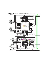
Page 44: ...44 MD P100 7 3 BLOCK DIAGRAM ...

Page 45: ...45 MD P100 ...

Page 46: ...der Fuse holder Orange lead wire extension cable Orange To terminal always supplied with power regardless of ignition switch position Tovehicle metal body Orange ToIP BUSoutput black This Product IP BUS cable Supplied with this product IP BUScable Supplied with the Multi CD player Head Unit With IP BUS input Multi CDplayer sold separately Connection Diagram ...

Page 47: ...th the buttons shown below Head Unit e g DEH P645R Remote Controller e g DEH P645R Operation is the same as when using buttons on the head unit FUNCTION button BAND button PGM button buttons PGM button Buttons 1 6 BAND button SO button buttons FUNCTION button ...

Page 48: ...yer starts playing Disc Number Track Search Press the or button to select the desired track Disc Search Press the or button to select the desired disc Disc Up Down Press the BAND button to select the desired disc Disc Up Disc Number Search You can select discs directly with the 1 to 6 buttons Just press the number corresponding to the disc you want to listen to Entering the Function Menu The Funct...

Page 49: ...ration and button for each function For details concerning an operation refer to the page indicated Multi MD Player Function name Display Button Operation Display Mode FUNC1 or Select Random Play FUNC2 or Hold for 2 seconds Select Scan Play FUNC3 or Select Repeat Play FUNC4 or Select Track Selection Mode or Select AUTO MANUAL Basic Operation ...

Page 50: ...tive type Max current consumption 0 8 A Dimensions 176 W 83 5 H 133 D mm Weight 1 2 kg System Mini disc digital audio system Usable discs Mini disc Frequency characteristics 20 20 000 Hz 1 dB Signal to noise ratio 95 dB 1 kHz IEC A network Output level 1 V 1 kHz 0 dB Number of channels 2 stereo ...

Reviews: