


ORDER NO.
PIONEER CORPORATION
1-1, Shin-ogura, Saiwai-ku, Kawasaki-shi, Kanagawa 212-0031, Japan
PIONEER ELECTRONICS (USA) INC.
P.O. Box 1760, Long Beach, CA 90801-1760, U.S.A.
PIONEER EUROPE NV
Haven 1087, Keetberglaan 1, 9120 Melsele, Belgium
PIONEER ELECTRONICS ASIACENTRE PTE. LTD.
253 Alexandra Road, #04-01, Singapore 159936
PIONEER CORPORATION
2011
2011 Printed in Japan
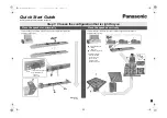
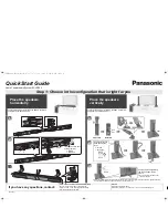
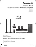
Center
Surround
Front
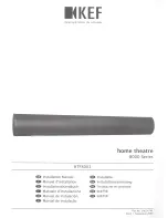
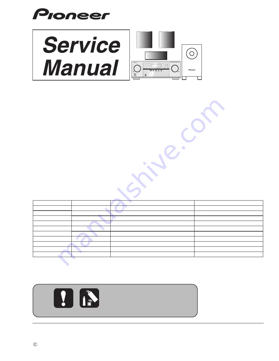
HTP-071
RRV4273
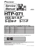
HOME CINEMA PACKAGE
HTP-071
AUDIO/VIDEO MULTI-CHANNEL RECEIVER
VSX-321-K-P
SUBWOOFER SPEAKER SYSTEM
S-22W-P S-11-P
HTP-071 is a Home Cinema Package and consists of VSX-321-K-P, S-22W-P and S-11-P.
THIS MANUAL IS APPLICABLE TO THE FOLLOWING MODEL(S) AND TYPE(S).
Model
HTP-071
SYXE8
AC 220 V to 230 V
HTP-071
CXE
AC 120 V
HTP-071
DLPWXE
AC 220 V to 240 V
HTP-071
AXE5
AC 220 V
VSX-321-K-P
SYXE8
AC 220 V to 230 V
VSX-321-K-P
CXE
AC 120 V
VSX-321-K-P
DLPWXE
AC 220 V to 240 V
VSX-321-K-P
AXE5
AC 220 V
—————
—————
—————
—————
S-22W-P
S-11-P
Type
Power Requirement
Remarks
K-IZ
V
OCT.
Summary of Contents for HTP-071
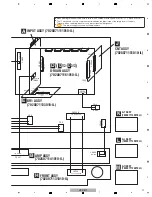
Page 9: ...9 HTP 071 5 6 7 8 5 6 7 8 A B C D E F ...
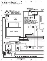
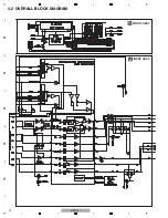
Page 12: ...12 HTP 071 1 2 3 4 A B C D E F 1 2 3 4 4 2 OVERALL BLOCK DIAGRAM H FRONT ASSY A INPUT ASSY ...
Page 89: ...89 HTP 071 5 6 7 8 5 6 7 8 A B C D E F C SIDE B CP1 CP3 CP5 CN1 CN3 ...
Page 93: ...93 HTP 071 5 6 7 8 5 6 7 8 A B C D E F D SIDE B CN600 CP104 ...