ORDER NO.
PIONEER ELECTRONIC CORPORATION
4-1, Meguro 1-Chome, Meguro-ku, Tokyo 153-8654, Japan
PIONEER ELECTRONICS SERVICE, INC. P.O. Box 1760, Long Beach, CA 90801-1760, U.S.A.
PIONEER ELECTRONIC (EUROPE) N.V. Haven 1087, Keetberglaan 1, 9120 Melsele, Belgium
PIONEER ELECTRONICS ASIACENTRE PTE. LTD. 253 Alexandra Road, #04-01, Singapore 159936
PIONEER ELECTRONIC CORPORATION 1999
c
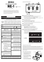
GR-209
RRV2147
1. SAFETY INFORMATION ...................................... 2
2. EXPLODED VIEWS AND PARTS LIST ................ 3
3. SCHEMATIC DIAGRAM ....................................... 6
4. PCB CONNECTION DIAGRAM ............................ 8
5. PCB PARTS LIST ............................................... 10
6. ADJUSTMENT .................................................... 10
7. GENERAL INFORMATION ................................ 11
7.1 IC .................................................................. 11
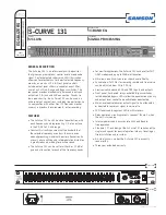
8. PANEL FACILITIES AND SPECIFICATIONS .... 13
CONTENTS
T – ZZR MAY 1999 Printed in Japan
THIS MANUAL IS APPLICABLE TO THE FOLLOWING MODEL(S) AND TYPE(S).
GRAPHIC EQUALIZER
Type
Model
Power Requirement
Remarks
GR-209
MYXCN1
AC220– 230V
SDXCN1
AC110/120–127/220/240V
With the voltage selector
209
STANDBY/ON