background image

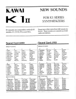
Summary of Contents for PM 5390 S

Page 1: ...RF synthesizer 0 1 MHz 1 GHz PM 5390 PM 5390 S 9452 053 90001 9452 053 90701 Service manual 9499 525 00811 8710 01 4 05 Industrial Electro acoustic Systems ...

Page 2: ...RF synthesizer 0 1 MHz 1 GHz PM 5390 PM 5390S 9452 053 90001 9452 q53 90701 Service manual 9499 525 00811 8710 01 4 06 PHILIPS ...

Page 3: ...rsonnel Maintenance and repairs may also be carried out only by qualified personnel Wichtig Da das Gerat ein elektrisches Betriebsmittei ist darf die Bedienung nur durch eingewiesenes Personal erfolgen Wartung und Reparatur durfen nur von geschultem fach und sachkundigem Personal durchgefiihrt werden Important Comme Tinstrument est un equipement eiectrique le service doit re assure par du personne...

Page 4: ... frequency generation 3 6 Power amplifier RF unit 12 PM 5390 S 3 7 Power supply unit 10 motherboard 4 access to PARTS 4 1 Dismantling the instrument 4 2 Fuse mains transformer 4 3 Carrying handle 4 4 Pushbuttons 4 5 RF OUTPUT connector 4 6 Unit 4 5 keyboard display interface 4 7 RF units 5 PERFORMANCE CHECK 5 1 General information 5 2 General functional test 6 SELF TEST PROGRAM DIAGNOSTIC PROGRAM ...

Page 5: ...er supply componeniMay out Fig 35 Unit 10 Unit 7 Motherboard Power supply circuit diagram Fig 36 Units U1 and U2 component lay out Fig 37 Unit 1 CPU lEC bus interface circuit diagram Fig 38 Unit 2 Control unit circuit diagram Fig 39 Unit 3 Modulation interface Fig 40 Unit 4 Keyboard display interface Fig 41 Unit 5 Keyboard display Fig 42 R F units mounted Fig 43 RF unit 1 component lay out Fig 44 ...

Page 6: ...ention to a potential danger that requires correct procedures or practices in order to prevent personal injury SYMBOLS Protective earth black grounding terminal IMPAIRED SAFETY PROTECTION Whenever it is likely that safety protection has been impaired the instrument must be made inoperative and be secured against any unintended operation The matter should then be referred to qualified technicians S...

Page 7: ......

Page 8: ...n OF THE BLOCK DIAGRAM fig 30 The instrument works under control of the 8085 microprocessor within the central processing unit CPU The program memory consists of two EPROMs On the data memory chip two further functions are implemented i e a timer generating sweep control signals and 12 output ports for the modulation modes on the modulation interface In the long term data memory up to 8 complete p...

Page 9: ...on signals are fed to the mixer oscillator VCO 3 in order to have a constant moclLi lation coefficient FM is only possible in the two lower frequency ranges up to 340 MHz as VCO is active in those ranges only The modulation interface unit 3 processes and matches the modulation signals for the RF units i e the Internal and external FM AM or VIDEO The different modes are controlled via port 1 on uni...

Page 10: ...mally the same software has to be replaced Please order loaded PROIvls directly via Philips Supply Center Service Hamburg The integrated circuit 318 is a multifunction chip with a RAM of 256 bytes two 8 bit and one 6 bit input output ports and a programmable timer The RAM memory is used by the processor as working storage Ports A and B send control signals from the processor to the modulation inte...

Page 11: ... switches 842 844 at the rear of the instrument serve for setting the I EC bus address Shift register 315 senses the states of the switches via the parallel inputs and gives this Information via the serial output to the serial address input ISR of 1C 305 When a data transfer via the I EC bus is started 1C 305 has to detect whether information received address corresponds to the address set by swit...

Page 12: ... from the port output B6 the output drives a relay which activates the 20 dB power amplifier in order to get a higher output amplitude of 1 Vrms Actuation is done by switching the amplifier supply voltage from 12 V to 24 V The remaining output lines of port 2 B7 and C0 C7 are used to control the coarse and fine attenuator in order to set the output amplitude from 127 dBm to 7 dBm The lines C5 C7 a...

Page 13: ...ator and the 23 1 divider 4 C 307 The division factor 23 1 is achieved by connecting the outputs of 1C 30 via NAND gate 31 1 to the reset input The function of the programmable divider and phase locked loop is further described in chapter 3 5 3 with fig 8 Another function on unit 2 is the sweep ramp generation The sweep time divider binary counter 312 counts pulses sent from the timer on unit 1 in...

Page 14: ...g 1 Unit 1 and 3 logic states of port outputs for modulation modes The sound part consists of a sound carrier oscillator modulator switched in during VIDEO a 1 kHz oscillator and an input circuitry for external internal sound signals for generation of AM and FM modu lation The 1 kHz oscillator is a RC oscillator based on the Wien bridge principle the components of which are 654 535 534 659 A recti...

Page 15: ...GLE and CONT are driven from the port outputs on the CPU unit 1 via the buffers 305 and 306 on U4 The information from the processor is fed to the keyboard controller via the data bus ADO AD7 data transfer is performed by the control signals RD WR Clk RES and IRQ The chip select signal CS is generated on the CPU card from the address decoder 1C 320 pin 7 Data information for the 7 segment displays...

Page 16: ...ugh to keep the oscillator frequency the same as the incoming frequency preserving the locked condition INPUT SIGNAL ViW A Hi OUTPUT SIGNAL Fig 2 Block diagram of Phase Locked Loop PLL Four of the six subranges 340 to 510 MHz 510 to 680 MHz 680 to 850 MHz and 850 to 1020 MHz are generated by VCO la d To get always the same dividing range N in loop 1 the output signal f1 of VCOl in this digital PLL...

Page 17: ... 5 MHz Reference frequency slow loop 1 fs 1 kHz Reference frequency fast loop 1 fF 10 kHz Reference frequency loop 2 and 3 fRef 39 0625 kHz Divider settings Ref divider for loop 1 A 5000 Divider 5 B 128 Progr divider for fs N 50 000 220 000 29x256 at 290 MHz Progr divider 2 n1 46 X 256 at 460 MHz 63x256 at 630 MHz 80x256 at 800 MHz Ref divider loop 3 n2 13056 The locked PLL loop 1 and 2 is represe...

Page 18: ...RF subrange Fig 5 RF unit 1 and 2 table of port settings ...

Page 19: ......

Page 20: ...s over which the loop will remain in lock Normally the lock range is centered at the free running frequency unless there is some non linearity in the system which limits the frequen cy deviation on one side fo The deviations from fo are referred to as the Tracking Range or Hold in Range Free Running Frequency fo coo Also called tne Center Frequency this Is the frequency at which the loop VCO opera...

Page 21: ... 8 Unit 2 Timing diagram HEF 4751 selected frequency 340 1 19 MHz The division factor N is set between 50 000 and 220 000 by the 6 prog inputs AO A3 B2 B3 in BCD code In a bit parallel digit serial format Divider 1 provides a fast output signal FF at output 27 which can have a phase jitter of 1 system input period to allow fast frequency locking The slow output signal FS at output 25 which is jitt...

Page 22: ...erature compensation is realized by NTC resistor 740 Coarse adjustment is achieved by a 100 dB attenuator In 10 dB steps at the RF output The 0 to 9 dB range of the pin diode attenuator is used for level setting from 7 dBm to 117 dBm PM 5390 S M3 dBm to 117 dBm while the 10 to 20 dB range is active from 1 17 to 127 dBm only The circuit diagram of the pin diode attenuator and the applied control vo...

Page 23: ...eration of the sweep time The set sweep time is converted by the processor into a division factor N of the timer circuit within 1C 318 U1 At each setting of a new frequency IRQ sweep see above the TCU signal increases the state of the binary counter 312 U2 by 1 6 output lines are connected to the summing point of the operational amplifier 304 via resistors 643 648 the values of which are binary we...

Page 24: ...10 Two stabilized 5 V voltages are generated by regulators 354 355 5A for the digital part of the units 1 2 3 10 and 5B for the keyboard display interface units 4 and 5 The display unit is separately supplied in order to have less influence by scan interference 12A is a stabilized voltage realized by the four terminal voltage regulator 351 it supplies RF units 1 and 2 Ground connections are conduc...

Page 25: ......

Page 26: ... outwards and take it off the cabinet Grip and arms of the carrying handle must be ordered separately see mechanical parts list A complete carrying handle can easily be constructed by pressing the arms into the grip Fig 11 Removing the carrying handle 4 4 PUSHBUTTONS For changing knobs for pushbuttons it is necessary to open the cabinet and remove unit 5 see 4 6 4 5 RF OUTPUT CONNECTOR Remove the ...

Page 27: ...nsolder the coax cable point 23 of unit 3 Remove the RF output connector piece 854 from progr attenuator loosen nut by spanner 8 mm PM 5390S from PA stage 81 5 Replug the RF connector fR of RF unit 1 Remove the RF output connector piece 883 loosen nut by spanner 8 mm Unsolder all connections to the motherboard of the RF unit except coax cables see table solder connections fig 42 Loosen the two jun...

Page 28: ...n 5 2 GENERAL FUNCTIONAL TEST Immediately after power being switched on a selftest routine is performed under which ROM and RAIVI are tested If a fault is detected a single numeric digit in the first place of the frequency field on the display indicates the location of the fault The rest of the display remains dark The numeric digits are assigned to the memories as follows 1 ROM 2 RAM 3 CMOS RAM A...

Page 29: ......

Page 30: ...gnostic program must be activated by replacing the built in program memory IC311 unit 1 of the CPU by the test PROM PM 5390 see fig 43 The instrument must be disconnected from the mains before The PROM must properly be inserted in the correct direction pins all in and not bent The test PROM PM 5390 should be ordered directly via PHILIPS Supply Centre Service Hamburg it has no service code number A...

Page 31: ...th 12th position read data decimal 4 Port test Key in 04 display 04 All output ports are set to high level unit 1 C 318 pins 21 35 and unit 2 ICs 305 309 pins 1 4 10 25 37 40 Pushing any key except ENTER effects alternating low and high level at all ports During high level the LEDs MOD INT EXT AM SWEEP SINGLE CONT are lighting LEDs FM and V IDEO are flashing simultaneously ENTER ends the test 5 lE...

Page 32: ...ly stated otherwise the voltage potentials refer to the relevant contact measured against measuring earth L RECOMMENDED TEST EQUIPMENT The following abbreviations are used for settings and for the test equipments X T o 20 dB Vac Vdc OSC C T SPA FAM PMTR CTV CTVS SV selected parameter mode or input keep setting concerned parameter not used output not terminated output terminated with 50 2 e g HP 10...

Page 33: ...8 28 mV 24 77 32 mV 23 76 35 mV 22 75 40 mV 21 74 45 mV 20 Volt dBm Volt 50 mV 19 25 mV 56 MV 18 28 mV CO CO 17 32 mV 71 mV 16 35 mV 79 mV 15 40 mV 00 D 14 45 mV 100 mV 13 50 mV 112 mV 12 56 mV 126 mV 11 63 mV 141 mV 10 71 mV 158 mV 9 79 mV 178 mV 8 89 mV CO CO 7 100 mV 0 22 mV 6 112 mV 0 25 mV 5 126 mV 0 28 mV 4 141 mV 0 32 mV 3 158 mV 0 35 mV 2 178 mV 0 40 mV 1 199 mV 0 45 mV 0 22 V 0 50 mV 1 25...

Page 34: ...X j Keyboard operation display indication after POWER ON Af 7 900 when ENTER key pressed flashing frequency display when ENTER key pressed For incorrect input keying and excee iing ranges see operating manual chapt 3 4 9 stacked command key in FREQ RECAlb ENTER 111 222 333 111 000 222 000 333 000 x1 x2 x3 Xl x2 x3 store parameter key in data STORE 1 3 recall memory key in RECALL 1 3 45 945 000 945...

Page 35: ... RF U1 R638 I RF U1 R638 and RF U12 R622 C520 I Output level coarse attenuator setting error incl frequency response adjustment range 0 5 dB if necessary iterate seq 4 1 setting error incl frequency response PM5390S adjustment range 0 5 dB C520 RF U 12 additional f 850 MHz 1 use for reference value seq 4 7 4 9 p coarse attenuator setting 10 dB steps or other UHF equipment 5 5 1 5 2 5 3 5 4 5 5 5 6...

Page 36: ...dc 2 35V at TP23 U3 AM mod depth signal to MOD IN r 2 20kHz 20Hz O 5Vpp 20kHz N 0 9vpp 2kHz 0 5Vpp AM int mod depth Af 38 5kHz 2kHz Af 38 5kHz 2kHz Af 75kHz 1kHz K 1 Af 26kHz 0 3kHz Af 26kHz 1kHz R677 U3 R675 U3 FM ext FAM setting FM P P 2 filter 10H2 200 kHz FM ext signal to MOD IN j 2kHz 0 5Vpp 20Hz 20kHz 0 5Vpp J 1kHz IVpp FM int FAM setting FM P P 2 filter 10HZ 200 kHz 5 5MHz_ 10kHz sound c O ...

Page 37: ...arrier int if neces repeat seq 8 6 AM sound carrier signal to MOD IN 5kHz 0 5Vpp FAM AM P P 2 filter 10Hz 2kHz freq 475 5MHz J_ AM sound carrier int if neces repeat seq 8 8 control video settings by colour TV CVBS pos polarity 1 Vpp into 75 2 Frequency sweep sweep period sweep time fly bacKt f ly backtime 200 ms 5MH if R626 U2 f Start sweep ramp f stop 1 50 X 1 MHz steps from 65 MHz up to 1 15 MHz...

Page 38: ...e detailed information in this part For final checks of the complete instrument the previous table 7 3 1 seq 1 0 10 must be used especially seq 4 1 5 8 output leve 1 RF units 1 and 2 are mounted to the connection board RF 813 All screening covers of the RF units must be closed and the specified wantiing up time must be finished ...

Page 39: ... 1b subrange 5 VCO 1c subrange 5 final frequency VCO 1c subrange 6 VCO Id subrange 6 final frequency VCO Id SV 50 IdBm ldB RF U1 R638 Vdc 4 5V 0 2V PMTR 7dBm 2dB RF U1 R697 PMTR 7dBm 2dB RF U1 C547 PMTR 7dBm 2dB RF U1 R721 PMTR 7dBiti 2dB RF U1 C595 PMTR 7dBm dB RF U1 R638 PMTR 7 dBm 2 Vdc 3 4V 50mV R681 U2 S 1 3 PMTR ref 2o 9 0 3dBm R681 U2 PMTR ref 2o 9 0 3dBm PMTR ref 1 0 2 0 2 dBm RF level adj...

Page 40: ...cs select some frequencies PM 539o PM539 OS check freq 190 MHz adjust by more less compression of coils check at freq 510 MHz adjust to minimum I base signal level oscillator VC02a ser LO 04 onw measured at IC303 pin 16 I base signal level oscillator VC02b ser LO 04 onw measured at IC303 pin 16 T residual FM FAM setting FM RMS filter 10Hz 3kHz check some freq e g 10 160 170 340 435 510 680 840 850...

Page 41: ...NG THE PROTECTIVE EARTH CONNECTION The correct connection and condition is checked by visual control and by measuring the resistance between the protective lead connection at the plug and the cabinet fra me The resistance shall not be more than 0 5 r2 During measurement the mains cable should be moved Resistance variations Indicate a defect CHECKING THE INSULATION RESISTANCE Measure the insulation...

Page 42: ......

Page 43: ...ly at a static free work station by qualified service personnel 9 3 HANDLING MOS DEVICES Though all our MOS integrated circuits incorporate protection against electrostatic discharges they can nevertheless be damaged by accidental over voltages In storing and handling them the following precautions are recommended CAUTION Testing or handling and mounting call for special attention to personal safe...

Page 44: ...eplacement take only specified components Do not use any adhesive to fix components Replaced chips must positioned flat on the pcb before soldering starts Use only resin core solder tin with silver 60 36 4 Ag Working method Carefully unsolder both soldering tags of the chip component Avoid to lift printed conductor on the pcb Remove all superfluous material Use a sucking iron or sucking copper llt...

Page 45: ...2 466 91448 20 17 5322 255 40336 21 3 5322 255 44107 22 1 5322 255 44055 23 4 5322 255 44229 24 2 5322 255 44234 25 6 5322 255 44235 501 1 4822 122 30128 601 1 4822 116 51279 760 1 5322 158 14034 1 5322 390 24013 5322 390 80129 COVER FOOT BOTTOM SIDE BEARING BUSH SPRING RATCHET RING FOR HANDLE ARM FOR HANDLE CARRYING HANDLE KNOB S MAINS CABLE S FUSE HOLDER FOOT REAR SIDE S MAINS TRANSFORMER until ...

Page 46: ...462732G PROM software version 315 INTEGR CIRCUIT HEF4014BD 482 2 209 10296 316 INTEGR CIRCUIT P8085AH 5322 209 50032 317 INTEGR CIRCUIT N74LS363N 5322 209 81776 318 INTEGR CIRCUIT P8155H 5322 209 14563 320 INTEGR CIRCUIT N74LS155N 4822 209 85752 321 INTEGR CIRCUIT ICL82 1 2CPA 5322 209 81775 DIODE S U1 401 402 DIODE AAZ15 482 2 130 30229 403 DIODE BAW62 4822 130 30613 404 DIODE AAZ15 482 2 130 302...

Page 47: ...4104 311 INTEGR CIRCUIT HEF4023BD 4822 209 10252 312 INTEGR CIRCUIT HEF4520BP 5322 209 14189 313 INTEGR CIRCUIT SN74LS05N 5322 209 84994 315 INTEGR CIRCUIT SN7409N 5322 209 84464 316 INTEGR CIRCUIT SN7406J 00 5322 209 86327 CAPACITORS U2 501 503 CAPACITOR CERAM 22PF 2 100V 4822 122 31063 502 CAPACITOR CERAM 22NF 80 63V 5322 122 31795 504 506 CAP ELEC SAL 10UF 20 16V 5322 124 14066 508 CAPACITOR CE...

Page 48: ...66 519 CAP ELEC SAL 22UF 20 6 3V 4822 124 20989 522 CAPACITOR CERAM 10NF 80 100V 482 2 122 30043 523 CAP ELECTROLYT 220UF 50 16V 4822 124 20693 531 CAP ELEC SAL 2 2UF 20 16V 4822 124 40902 532 CAP ELEC SAL 47UF 20 6 3V 4822 124 40901 533 535 CAPACITOR FOIL 100NF 10 50V 5322 122 30108 541 CAP ELECTROLYT 47UF 20 10V 5322 124 21391 542 550 CAPAITOR CERAM 220PF 10 100V 4822 122 30094 543 549 CAP ELECT...

Page 49: ...37 377 TRANSISTOR BC338 4822 130 44121 378 379 TRANSISTOR BC558B 4822 130 44197 380 381 TRANSISTOR BC636 4822 130 44283 382 383 TRANSISTOR BC558B 482 2 130 44197 384 389 TRANSISTOR BC636 4822 130 44283 INTEGRATED CIRCUITS U4 301 INTEGR CIRCUIT N74LS154N 5322 209 86085 302 INTEGR CIRCUIT P8279 5322 209 86243 303 INTEGR CIRCUIT SN74LS03N 5322 209 85265 304 INTEGR CIRCUIT N74LS155N 5322 209 85752 305...

Page 50: ...2 209 86026 CAPACIT0RS U10 503 CAP ELECTROLYT 47UF 50 63V 482 2 124 20733 504 CAP ELECTROLYT 220UF 50 63V 4822 124 20801 505 CAP ELECTROLYT 10UF 50 63V 5322 124 21356 506 CAP ELECTROLYT 4 7UF 50 63V 4822 124 20726 507 511 CAP ELEC SAL 1 5UF 20 25V 482 2 124 20942 508 512 CAP ELECTROLYT 22UF 50 25V 4822 124 20698 509 513 CAPACITOR CERAM 10NF 50 100V 4822 122 31414 510 CAP ELECTROLYT 6800UF 30 25V 5...

Page 51: ... DIODE REFERENCE BZX79 B5V6 4822 130 34173 421 423 DIODE BA379 5322 130 80399 424 DIODE BA482 5322 130 34955 425 426 DIODE BA379 5322 130 80399 427 DIODE BAW62A 4822 130 30613 428 DIODE BA379 5322 130 80 399 431 435 DIODE BAW62 4822 130 30613 437 DIODE BB405B 5322 130 34953 438 DIODE BAT85 2 diodes 4822 130 31983 LO 05 onw 441 DIODE BA379 5322 130 80399 INTEGRATED CIRCUITS RF U1 301 302 INTEGR CIR...

Page 52: ...1998 509 CAPACITOR CHIP 820PF 80 400V 5322 122 32001 510 511 CAPACITOR CERAM 22NF 80 63V 5322 122 31795 512 513 CAPACITOR CHIP 820PF 80 40 0V 5322 122 32001 515 CAPACITOR CERAM INF 10 63V 5322 122 40419 516 517 CAPACITOR CHIP INF 10 63V 5322 122 31998 518 CAPACITOR CERAM 56PF 2 63V 5322 122 40408 519 CAPACITOR CHIP INF 10 63V 5322 122 31998 520 524 CAPACITOR CERAM INF 10 63V 5322 122 40418 521 523...

Page 53: ...CAPACITOR CHIP 220NF 10 63V 5322 122 31999 594 CAPACITOR CERAM 56PF 2 63V 5322 122 40408 595 CAPACITOR TRIMM 20PF 2PF 4822 125 50201 596 CAPACITOR CHIP 820PF 80 400V 5322 122 3200 1 599 CAPACITOR TRIMM 3 8PF 5322 125 60097 RESISTORS RF U1 600 RESISTOR CARBON 10E 5 0 2W 4822 116 52176 625 628 RESISTOR CARBON 16E 5 0 2W 4822 111 30712 629 660 RESISTOR CARBON 51E 5 0 2W 4822 111 30769 638 POTM TRIMMI...

Page 54: ...304 INTEGR CIRCUIT 305 INTEGR CIRCUIT 306 INTEGR CIRCUIT 307 INTEGR CIRCUIT 308 INTEGR CIRCUIT 309 310 INTEGR CIRCUIT 311 INTEGR CIRCUIT 312 INTEGR CIRCUIT 313 INTEGR CIRCUIT 314 INTEGR CIRCUIT 315 INTEGR CIRCUIT 321 INTEGR CIRCUIT 322 INTEGR CIRCUIT 323 INTEGR CIRCUIT 323 INTEGR CIRCUIT see info fig CAPACIT0RS RF U2 481 482 483 487 488 495 496 501 502 503 CAP FEEDTROUGH CAP FEEDTROUGH CAP FEEDTRO...

Page 55: ...ERAM 22NF 80 63V 5322 122 31795 561 CAPACITOR FOIL 220NF 10 100V 4822 121 40232 562 CAPACITOR CERAM 12PF 2 63V 5322 122 40404 563 CAPACITOR TRIMM 2 5 27P 100V 5322 125 54083 564 CAPACITOR CERAM 220PF 2 63V 5322 122 40407 565 CAPACITOR CERAM 120PF 2 63V 5322 122 40406 566 567 CAPACITOR CERAM INF 10 63V 5322 122 40419 570 571 CAPACITOR CERAM 4 7NF 10 100V 4822 122 30128 572 CAPACITOR CERAM 22NF 80 6...

Page 56: ...H 2 2NF 80 160V 5322 122 70115 34 36 CAP FEEDTROUGH 47PF 10 160V 5322 122 70113 40 43 CAP ELEC TANTAL 10UF 50 16V 5322 124 14066 532 CAP ELECTRLYT 68UF 50 16V 4822 124 20689 533 CAPACITOR FOIL 47 ON 10 5322 121 41884 RF UNIT 10 DIODES RF U10 401 402 DIODE BA244 5322 130 34794 CAPACITORS RF U1 0 501 504 CAPACITOR CERAM 18PF 2 63V 5322 122 40421 502 503 CAPACITOR CERAM 39PF 2 63V 5322 122 40422 RF U...

Page 57: ...onw 530 CAP FEEDTROUGH FKE350 5322 121 44228 RESISTORS RF U1 2 601 RESISTOR CHIP 4E7 10 0 1 25W 5322 111 90376 602 606 RESISTOR CARBON IK 5 0 2W 4822 111 30269 607 RESISTOR M FILM 1E78 1 0 4W 5322 116 51755 610 615 RESISTOR IK 5 0 2W 4822 111 30269 619 RESISTOR CARBON 16E 5 0 2W 4822 111 30712 620 RESISTOR CARBON 270E 5 0 2W 4822 116 52217 622 633 RESISTOR CARBON 360E 5 0 2W 4822 111 30746 624 RES...

Page 58: ......

Page 59: ...2 52 3 4443 53 6 4444 54 9 4445 56 2 4446 57 6 4447 59 4448 60 4 4449 61 9 4451 63 4 4375 64 9 4453 66 5 4454 68 1 4455 69 8 4456 71 5 4457 73 2 4458 75 4459 76 8 0494 78 7 0578 80 6 4461 82 5 4462 84 5 4463 86 6 4464 88 7 4465 90 9 4466 93 1 4467 95 3 0569 97 6 4468 100 4469 102 4471 105 4472 107 4473 110 4474 113 4475 115 4476 118 4477 121 4426 124 4478 127 4479 130 4481 133 4482 137 4483 140 44...

Page 60: ...3 29 K4 4654 30K1 4655 30K9 4656 31 K6 4657 32K4 4658 33 K2 0482 34K 4659 34K8 4661 35K7 4662 36K5 0726 37 K4 4663 38K3 0483 39K2 4664 40K2 4666 41 K2 4666 42K2 0474 43 K2 4667 44K2 4668 45 K3 4669 46 K4 0557 47 K5 4671 48K7 0442 49K9 0674 51K1 0672 52K3 4673 53K6 4674 54K9 4675 56K2 4676 57K6 4677 59K 4678 60K4 4679 61 K9 0872 63 K4 4681 64K9 0514 66K5 4682 68K1 4683 69 K8 4684 71 K5 4685 73 K2 0...

Page 61: ...C2 digital phase comparator output MOD phase modulation input OL out of lock indication OSC reference oscillator buffer input XTAL reference oscillator buffer output Aq to Ag programming inputs programmable NSq N i divider programming inputs prescaler OUT reference divider output 7Z84472 Fig 1 Pinning diagram HEF4750VD 28 lead DIL ceramic cerdip SOT 135A I I crystal standard external circuitry 7Z8...

Page 62: ...al programme The decade selection address is generated by an internal programme counter which may run continuous ly or on demand Two or more universal dividers can be cascaded each extra U D in slave mode adds two decades to the system The combination retains the full programmability and features of a single U D The U D provides a fast output signal FF at output OFF which can have a phase jitter o...

Page 63: ......

Page 64: ...11 4 j H L test state HIGH state the more positive voltage LOW state the less positive voltage _state is Immaterial ...

Page 65: ... is achieved with a 50 duty cycle Each of the Mode Control inputs is connected to an internal 2 k resistor with the other end uncom mitted RM j and RM2 An M input can be driven from a TTL circuit operating from the same Vqq by connecting the free end of the associated 2 k resistor to When an M input is driven from an ECL circuit the 2 k resistor can be left open or if required can be connected to ...

Page 66: ...n 15 to the internal Vg0 reference By connecting this to the CP input as shown in Figure a the clock Is automatically centered about the input threshold A clock duty cycle of 50 provides the fastest operation since the flip flops are master slave types with offset clock thresholds between master and slave This feature ensures that the circuit will operate with clock waveforms having very slow rise...

Page 67: ... pulse for every 10 pulses of f 2 Treated as a system building block the overall divide ratio N can be expressed as follows Pulse swallowing has been described as a way of combining a counter that is very fast but rather dumb with a counter that is very smart but rather slow to make the rest of the logic think that there is a very fast very smart counter up front For purposes of discussion a smart...

Page 68: ...of the switch while a program counter provides the net out put f 3 which also serves as a Preset control At the beginning of a cycle the switch selects the upper prescaler After S pul ses of swallow counter throws the switch to thelt wer prescaler output Still later the program counter reacihes maximum and causes a Preset This in turn causes the swa ow counter to throw the switch back to the upper...

Page 69: ... prescalers have divide ratios such as 1 O 1 1 and 5 6 U and L differ only by one and changing S by a certain amount changes N by the same amount Thus the combination of the prescaler and the swallow counter actsHke a single very fast fully programmable divider A similar analysis with M as the variable shows that the smallest ad justment afforded by the program counter is L N U L S L M 1 U L S LM ...

Page 70: ...tem 75 If units are not numbered do not fill in the four boxes see Example Job sheet relevant box Component sequence no Category These six boxes are intended to pinpoint the faulty component A Enter the component designation as used in the circuit diagram If the designation is alfa numeric the letters must be written starting from the left in the two left hand boxes and the figures must be written...

Page 71: ...data bus RF OUTPUT MOD IN Fig 30a Basic principle of operation Fig 30 Block diagrann Blockschaltbild Schema synoptique ...

Page 72: ...Fig 31 Front view Fig 32 Rear view ...

Page 73: ...L J ...

Page 74: ...U7 Fig 34 Unit 10 Unit 7 Motherboard Power supply ...

Page 75: ...oav ...

Page 76: ... see table 7 3 1 seq 5 2 F E D Fig 36 Units U1 and U2 component lay out ...

Page 77: ......

Page 78: ......

Page 79: ......

Page 80: ...602 ...

Page 81: ...Unit 5 Keyboard display ...

Page 82: ... RF board RFUnit2 colour violet 10 kHz brown orange black brown yellow green ye llow orange RF units mounted colour comp yjgigil m 9 nm mBBB m 1 yellow mBMW mB m coax Dmm HHI HI SSI 5 VCO 1C IIHM 3 VC0 1D mbbqi 1 R615 1 BtSifksusil iMa immmi ...

Page 83: ......

Page 84: ...f to mixerl U2 RF from U3 AM Video from D A converter U2 VR2 Fig 44 RF unit 1 ...

Page 85: ...use special soldering tin housing of components must be fixed to pcb O O ioioioZ 8 O O PHILIPS I ISoSoSoSoSoS SoSoSoSoSi O O Fig 45 RF unit 2 component lay out ...

Page 86: ...ts MOD Vqq phase comp in 314 PCI HEFW50 loop filter I 578 I 1 lOOn I 0678 L U L Frequency synthesizer OUT R ISA 573 J574 J575 16n JOn 6 5 Neu I I 4 i FR96 __533 VC0 2b H Prescaler 256 1 633 546 360R II In progr divider 2 597 II 12pF 308 HEFiOW LIMJJJ 661 5 MHz ref oscillator 666 l 54ff J J566 C548B Jin T 751 IsMHzTyynr J p J 30 2 548 638 HI divider 5 128 1 jS50 J551 S JOOpJ22n Jo Vqq 12 Pin16 Vgs ...

Page 87: ......

Page 88: ... 615277 612799 service New Zealand Philips New Zealand Ltd Scientific and Industrial Equipment Division 68 86 Jervois Quay G P O Box 2097 Wellington Cl tel 64 4 735735 Nigeria Associated Electronic Products Nigeria Ltd KM16 Ikorodu Road Ojota P O B 1921 Lagos tel 234 1 900160 69 Nippon NF Trading Co Ltd 3 20 Tsunashima Higashi 6 Chome Kohoku ku Yokohama Shi Norge Norway Norsk A S Philips Dept Indu...

Reviews: