


GB
CLASS 1
LASER PRODUCT
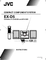
COMPACT
DIGITAL AUDIO
Service
Service
Service
Service
Service
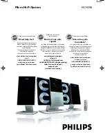
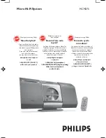
MCM275
TABLE OF CONTENTS
©
Copyright 2006 Philips Consumer Electronics B.V. Eindhoven, The Netherlands
All rights reserved. No part of this publication may be reproduced, stored in a retrieval system or
transmitted, in any form or by any means, electronic, mechanical, photocopying, or otherwise
without the prior permission of Philips.
Published by SL 0733 Service Audio
Printed in The Netherlands
Subject to modification
Micro System
3141 785 30334
Version 1.4
Service Manual
all versions
From week 714 onwards, the CD Mechanism was changed to
Dayang M93. New CD & MCU Board was used to match with
the new CDM.
Please refer chapter 1 to 9 for sets produced before week 713 and
chapter 11 for sets produced in or after week 714.
Revision List ...........................................................................P11-1
Summary of Contents for MCM 275
Page 16: ...4 1 4 1 SET BLOCK DIAGRAM ...
Page 17: ...5 1 5 1 SET WIRING DIAGRAM ...
Page 23: ...LAYOUT DIAGRAM MAIN BOARD 5757 for 37 98 TOP SIDE 6 6 6 6 ...
Page 24: ...6 7 6 7 LAYOUT DIAGRAM MAIN BOARD 5757 for 37 98 BOTTOM SIDE ...
Page 25: ...CIRCUIT DIAGRAM MAIN BOARD 5757 for 37 98 6 8 6 8 ...
Page 26: ...6 9 6 9 LAYOUT DIAGRAM MAIN BOARD 5762 for 05 12 TOP SIDE ...
Page 27: ...LAYOUT DIAGRAM MAIN BOARD 5762 for 05 12 BOTTOM SIDE 6 10 6 10 ...
Page 28: ...CIRCUIT DIAGRAM MAIN BOARD 5762 for 05 12 6 11 6 11 ...
Page 32: ...LAYOUT DIAGRAM CD MCU BOARD TOP SIDE 7 2 7 2 ...
Page 33: ...7 3 7 3 LAYOUT DIAGRAM CD MCU BOARD BOTTOM SIDE ...
Page 34: ...7 4 7 4 CIRCUIT DIAGRAM CD MCU BOARD CD PORTION ...
Page 35: ...CIRCUIT DIAGRAM CD MCU BOARD MCU PORTION 7 5 7 5 ...
Page 36: ...LAYOUT DIAGRAM SW BOARD TOP SIDE 7 6 7 6 LAYOUT DIAGRAM SW BOARD BOTTOM SIDE ...
Page 38: ...LAYOUT DIAGRAM AC POWER BOARD TOP SIDE 8 2 8 2 LAYOUT DIAGRAM AC POWER BOARD BOTTOM SIDE ...
Page 39: ...8 3 8 3 CIRCUIT DIAGRAM AC POWER BOARD ...
Page 45: ...9 1 9 1 SET MECHANICAL EXPLODED VIEW 1 ª º 2 4 7 8 9 3 5 6 ...
Page 47: ...9 1 9 1 SET MECHANICAL EXPLODED VIEW 1 ª º 2 4 7 8 9 3 5 6 ...
Page 48: ...10 2 10 2 LAYOUT DIAGRAM CD MCU BOARD TOP VIEW ...
Page 49: ...10 3 10 3 LAYOUT DIAGRAM CD MCU BOARD BOTTOM VIEW ...
Page 50: ...10 4 10 4 CIRCUIT DIAGRAM CD MCU BOARD CD PORTION ...
Page 51: ...10 5 10 5 CIRCUIT DIAGRAM CD MCU BOARD MCU PORTION ...