background image

Published by Sophie-KM 1135 AVM

Printed in the Netherlands

MCD2010/12/93/98

Subject to modi cation

EN

Micro Audio System

Contents

Page

Contents

Page

©Copyright 2011 Philips Consumer Electronics B.V. Eindhoven, The Netherlands.
All rights reserved.  No part of this publication may be reproduced, stored in a 
retrieval system or transmitted, in any form or by any means, electronic, 
mechanical, photocopying, or otherwise without the prior permission of Philips.

Version 1.0

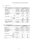
1 Technical Specification and Connection Facilities

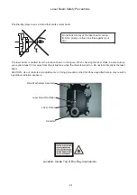
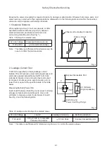
2  Laser Beam Safety Precautions......................................... 2-1

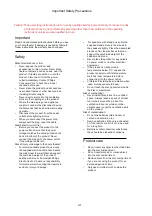
3  Important Safety Precautions .................................. 3-1 to 3-2

4  Safety Check After Servicing ............................................. 4-1

6  Standard Notes For Servicing,Lead Free Requirements
    & Handling Flat Pack IC .......................................... 6-1 to 6-4

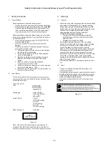
5  Safety Information General Notes & Lead Free

7  Direction of Use ....................................................... 7-1 to 7-4

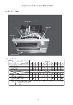
8  Cabinet Disassembly Instructions ........................... 8-1 to 8-2

12  Headphone Board

9 Troubleshooting ....................................................... 9-1 to 9-2

10  Block Diagram .................................................................10-1

11  Wiring Diagram ...............................................................11-1

13  Display Board

14  Power Board

Layout Diagram.................................................12-5

16   Exploded View...................................................................13-1

17  Revision List .......................................................................14-1

15  Decoder Board 

Circuit Diagram ......................................... 12-6 to 12-11

Layout Diagram ............................................... 12-12

.................................................1-1 to 1-10

Circuit Diagram ....................................................12-1

Layout Diagram ...................................................12-1

Circuit Diagram ................................................12-2

Circuit Diagram .................................................12-4

Layout Diagram ...............................................12-3

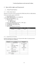
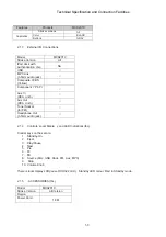
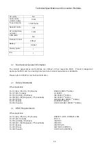
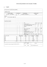
Requirements .................................................................... 5-1

Features

RDS

Voltage Selector
ECO Standby

DTS

Feature

Different

/12

/93 /98

/10


3141 785 36600

Summary of Contents for MCD2010/12/93

Page 1: ...tant Safety Precautions 3 1 to 3 2 4 Safety Check After Servicing 4 1 6 Standard Notes For Servicing Lead Free Requirements Handling Flat Pack IC 6 1 to 6 4 5 Safety Information General Notes Lead Free 7 Direction of Use 7 1 to 7 4 8 Cabinet Disassembly Instructions 8 1 to 8 2 12 Headphone Board 9 Troubleshooting 9 1 to 9 2 10 Block Diagram 10 1 11 Wiring Diagram 11 1 13 Display Board 14 Power Boa...

Page 2: ...oard TIPS C Component Lever Repair M Module Lever Repair Used 55 55 58 58 61 61 79 79 93 93 94 94 96 96 98 98 51 37 12 12 10 10 Feature diffrence RDS DTS VOLTAGE SELECTOR ECO STANDBY DARK Type Versions MCD2010 Technical Specification and Connection Facilities 1 1 C C M M C C M M C C M M Decoder Board CD Loader Display Board Headphone Board Power Board ...

Page 3: ...nt of the set 5 Tuner FM Silicon Lab SI4705 w RDS 6 Digital Amplifier 7 Rated output power 10 THD table 2 Set Type Number Stroke Versions Power Remark MCD2010 All version 2x10W 2 1 2 Styling Forms and Functions MCD2010 appearances are defined in their respective MUS MUS is the leading document where product appearance is applicable Features Products MCD2010 Stroke versions l l A Design Refer to MU...

Page 4: ...Out RCA cinch Tuner Socket for FM Headphone Out 3 5mm audio jack 2 1 4 Controls Local Displa y and LED Indications tbc Control keys on the set are 1 Standby On 2 Eject 3 Play Pause 4 Next 5 Pre 6 FF 7 FB 8 Source Disc USB Dock FM Aux MP3 9 Stop 10 Volume Knob There is local display LCD reuse DCD322 LCD Standby LED colour Red in Standby mode 2 1 5 ACCESSORIES tbc Model MCD2010 Stroke Version All Ve...

Page 5: ... Standards Where applicable For 12 EU 05 UK 51 Russia EN IEC 60065 7th Edition For 37 US Canada UL 60065 For 55 LATAM 78 Brazil IEC 60065 7th Edition For 98 AP 69 Singapore 75 Australia IEC 60065 7th Edition For 93 China GB 8898 IEC 60065 7th Edition For 61 Korea K 60065 6th Edition For 96 Taiwan CNS 14408 IEC 60065 7th Edition 2 4 EMC Requirements Where applicable For 12 EU 05 UK 51 Russia EN5501...

Page 6: ...or positive and negative polarity for unit on and off for 1kV incremental steps 2 Component or mechanical damage is not allowed No loss of fixed stored data stored in EEPROMs 3 Hang ups and malfunctions are allowed as long as the customer can recover from the hang up by pressing the Standby or ON OFF button of the set 4 Failures that disappear only by unplugging the AC mains cord and or power sour...

Page 7: ...8 9 94 India 2 100 310Vac limit India compatible with up cost used only for India Frequency 47 63Hz EU 12 round 2 pin All requirements per defined for each country should be met with sufficient testing 3 1 2 Surge Immunity Lightning Test The product shall withstand mains interference s of Differential mode 2kV 2 ohm criteria C for Europe 6kV 12 ohm criteria C for NAFTA Parameters Bi wave Open circ...

Page 8: ...rmance criterion B Variation 0 100 dip at T event 5 Sec Performance criterion C Additional for USA apparatus See 3135 019 8029 Reliability evaluation Variation 0 100 dip at T event 100 mSec in standby mode Performance criterion B Requirement No misoperation and no interference of user in order to guarantee continuation of performed function Reference IEC61000 4 11 For measuring method refer to UAN...

Page 9: ...tput 1 Tuner FM 67 5kHz Modulation Limit 6dB Line Out Left Right 2000mV 200mV CD MP3 3dB track Audio Disc 1 Track 1 Headphone 15mW 2 dB RL 32Ω S H 0 2 e v a w e n i s z H K 1 B d 3 B S U AUX1 back 1V Rin 22kΩ MP3_link front 750mV Rin 22kΩ IPOD Docking 750mV Rin 22kΩ Output Power 1 At THD 10 1kHz sinewave MCD2010 Main Operation for all version rms 10W 1dB At Cold Condition with 10 THD Tuner output ...

Page 10: ... luminance delay 2T pulse 20ns 20ns Subcarrier locked unlocked 75 Color bar locked locked k c a l B 0 l e v e L C D 1V 1V 3 2 2 2 Component Video Y Pb Pr Description Test Signal Specification Interlace Progressive NTSC PAL 0 1 V m 0 0 0 1 0 1 V m 0 0 0 1 e t i h W 0 0 1 t u p t u o e d u t i l p m A 0 1 V m 0 0 7 0 1 V m 4 1 7 e t i h W 0 0 1 r a b e t i h W PbPr peak to peak 75 Color bar 525mV 10...

Page 11: ... t a c i f i l p m A 3 2 z H k 5 7 v e D q r F V m 1 F R n o i t r o t s i D Overall Frequency Response 63Hz 12 5KHz 3 dB Channel separation 400 1000 5000 Hz RF input 68 dBf 26 30 20 20 26 18 dB Frequency MHz Noise Limited Sensitivity 26 dB Image Rejection IF Rejection Large Signal Handling Selectivity S9 300 kHz 2 2 0 0 0 1 4 6 0 3 8 1 m o N M F 1 8 1 0 0 5 5 4 5 2 2 2 m i L 0 8 8 2 2 0 0 0 1 4 6...

Page 12: ...the pickup lens when the diode is turned on Do not look directly at the laser beam CAUTION Use of controls and adjustments or doing procedures other than those specified herein may result in hazardous radiation exposure Location Inside Top of Blu Ray mechanism Do not look directly at the laser beam coming from the pickup or allow it to strike against your skin Drive Mechanism Assembly Laser Beam R...

Page 13: ... Important Important Safety Precautions Read and understand all instructions before you use your home theater If damage is caused by failure to follow instructions the warranty does not apply Safety Riskof electricshock or fire Never expose the product and accessories to rain or water Never place liquid containers such as vases near the product If liquids are spilt on or into the product disconnec...

Page 14: ...ic products Please act according to your local rules and do not dispose of your old products with your normal household waste Correct disposal of your old product helps to prevent potential negative consequences for the environment and human health Your product contains batteries covered by the European Directive 2006 66 EC which cannot be disposed with normal household waste Please inform yoursel...

Page 15: ... and externally exposed accessible parts RF terminals antenna terminals video and audio input and output terminals microphone jacks earphone jacks etc is lower than or equal to the specified value in the table below Measuring Method Power ON Insert load Z between B earth ground power cord plug prongs and exposed accessible parts Use an AC voltmeter to measure across the terminals of load Z See Fig...

Page 16: ...e sure that during repair you are at the same potential as the mass of the set by a wristband with resistance Keep components and tools at this same potential Available ESD protection equipment Complete kit ESD3 small tablemat wristband 4822 310 10671 Wristband tester 4822 344 13999 Be careful during measurements in the live voltage section The primary side of the power supply including the heatsi...

Page 17: ...older paste is required please contact the manufacturer of your solder equipment In general use of solder paste within workshops should be avoided because paste is not easy to store and to handle Use only adequate solder tools applicable for lead free solder alloy The solder tool must be able To reach at least a solder temperature of 400 C To stabilize the adjusted temperature at the solder tip To...

Page 18: ... this and more technical information within the magazine chapter workshop news For additional questions please contact your local repair helpdesk How to Remove Install Flat Pack IC 1 Removal With Hot Air Flat Pack IC Desoldering Machine 1 Prepare the hot air flat pack IC desoldering machine then apply hot air to the Flat Pack IC about 5 to 6 seconds Fig S 1 1 2 Remove the flat pack IC with tweezer...

Page 19: ...e flat pack IC you can remove it easily Fig S 1 3 2 Affix the wire to a workbench or solid mounting point as shown in Fig S 1 5 3 While heating the pins using a fine tip soldering iron or hot air blower pull up the wire as the solder melts so as to lift the IC leads from the CBA contact pads as shown in Fig S 1 5 4 Bottom of the flat pack IC is fixed with glue to the CBA when removing entire flat ...

Page 20: ...lectrostatic charge during unpacking or repair work 1 Ground for Human Body Be sure to wear a grounding band 1 M that is properly grounded to remove any static electricity that may be charged on the body 2 Ground for Workbench Be sure to place a conductive sheet or copper plate with proper grounding 1 M on the workbench or other surface where the semi conductors are to be placed Because the static...

Page 21: ... next track title or file Select a programmed radio station Disc compartment Hold the disc USB socket MP3 LINK Connect external audio device Headphone socket Turn on the apparatus switch to standby mode or Eco Power standby mode IR sensor Detect signals from the remote control Always point the remote control at the IR sensor Display panel Show current status Open or close the disc tray VOLUME Adju...

Page 22: ...n a track or disc Fast backward or forward For menus navigate left right Rotate a picture Adjust time OK 8 9 10 11 12 13 14 15 Return to a previous display menu Start pause or resume play Skip to the previous next track title or file Adjust the volume Select a title chapter track to play Program radio stations Set clock Set sleep timer Set alarm timer Mute Select a programmed radio station VOL Num...

Page 23: ...stening position Connect Connect speakers 1 Insert the speaker wires completely into the speaker input sockets on the back of the unit Option 2 Connect through component video cables Connect a progressive scan TV through component video cables for higher quality video Connect power Caution Risk of product damage Ensure that the power supply voltage corresponds to the voltage printed on the back or...

Page 24: ...oduct the audio output sockets on the external device for example audio player Connect FM aerial Tip For optimal reception fully extend and adjust the position of the antenna For better FM stereo reception connect an outdoor FM antenna to the FM AERIAL socket The unit does not support MW radio reception 1 Connect the supplied FM antenna to the FM AERIAL socket on the main unit AUX OUT ...

Page 25: ...he part 3 Figure Number for reference 4 Identification of parts to be removed unhooked unlocked released unplugged unclamped or desoldered Axx Screw CNxx Jxx CONxx Connector D3 5X12BA is specification of screw Unhook Unlock Release Unplug or Desolder e g 7 A01 seven Screws Fig D1 Fig D2 Fig NO Remove Unhook Unlock Release Unplug Desolder Note 3 Decoder Board Power Board Video Output Board D3 4 CD ...

Page 26: ...8 2 Fig D4 Cabinet Disassembly Instructions ...

Page 27: ...d circuit check and change the related components of radio controlled circuit check if power supply of radio is normal check and change related components of power supply circuit check if radio circuit components of around it is normal check and change components of around it No No No No No No No sound from whole unit FLOW CHART NO 3 Yes No Yes No Yes no sound from DVD check if DVD output is norma...

Page 28: ... wire is broken check and change video wire socket No display from display screen check if video socket video wire is normal Decoding is broken check if tie wires of laser head ass y is loosen and broken laser head ass y broken no image from DVD change capacitance change display screen check if display screen is broken Yes check if the capacitor voltage of filaments filter is short circuit Yes che...

Page 29: ...N LCD BUS Stb clk data MCU3 3V M3 3V Seg grid BUS 5V DRIVER DRV632 AMP JDA7491HV M3 3V BD3491 3490 BD3491FS FR_OUT AMPLIFIER TDA7491HV TDA7492P FL_OUT LCD Controller ET8862 HT1622 MCU R5F21266 IR IR AD_KEY EEPROM M24C02 Apple Ceriticiate CP2 0B STB MUTE STB MUTE TX RX CTL DET M3 3V 6 OHM_10W 20W 25W 2 TX RX CTL DET DVD_ON VUSB_ON DC DC AP1501 9435 DVD_5V 12V 18V AMP JDA7491HV S3 3V F3 3V E3 3V TRA...

Page 30: ...W4 SW5 SW2 PJ4 IR EC2 LED1 SW3 LED2 J9 PJ5 ECO_POWER GND CON3 PJ2 CON1 Headphone Board Video Output Board CON2 USB CON5 J13 RCA1 RAC2 Display Board DVD Loader CON2 3 5V GND GND 12V 12V CON1 Power Board CON4 CON3 U12 CON5 J1 J2 P1 U5 HA1 CN1 J5 U7 U6 J4 J7 J3 CON6 Decoder Board 11 1 11 1 ...

Page 31: ...01 R1 47K C1 103 1 1 2 2 3 3 CON1 CON2 0 3 2 0 3P R2 47K C2 103 FB1 600R FB2 600R 1 1 2 2 3 3 4 4 CON3 C3 100P C4 100P 1 3 2 11 10 PJ2 A JP CK3511 PJ2 B PJ2 C MP3_L AGND MP3_R PGND H_OUTR H_OUTL PH MUTE 1 VCC 2 D 3 D 4 GND USB 1 2 3 4 5 CON2 DGND D D VBUS 12 1 12 1 ...

Page 32: ...G11 33 COM5 32 COM6 31 COM7 30 COM8 29 SG29 28 SG28 27 SG27 26 SG26 25 SG25 24 SG24 23 SG23 34 COM4 35 COM3 36 COM2 37 COM1 38 VLCD 39 VSS 40 OSC 41 VDD 42 CE 43 CLK 44 DI 22 SG22 21 SG21 20 SG20 19 SG19 18 SG18 17 SG17 16 SG16 15 SG15 14 SG14 13 SG13 12 SG12 U1 I PT6533 EC6 EC 100UF 10V R35 10R C15 100P C7 102 R36 43K C8 100P R4 100R R3 100R R23 100R J1 J2 J3 J4 J5 AD1 AD2 IR 3 3V A5 6V ECO_POWER...

Page 33: ...Display Board Layout Diagram 12 3 12 3 ...

Page 34: ...PF 50V C4 0 1uF 25V C10 0 1uF 25V D5 FR107 D6 FR107 D7 NC D10 SB260 Q1 4N60C EC3 22uF 50V IC2A PC817 IC2B PC817 EC5 470uF 10V EC4 470uF 10V L1 10uH U1 TL431 Z2 NC EC7 1000uF 25V EC6 1000uF 25V EC8 470uF 25V L2 10uH R16 1K L N R37 1M R36 1M D1 D2 D3 D4 1N4007 1N4007 1N4007 1N4007 EE25 C11 102 1kV 1 2 3 4 CON2 4P 2 0 12V 3 5V GND GND 1 4 3 5 6 7 8 9 R34 1M R35 1M D8 MBR10100C R23 33R R24 33R C9 102 ...

Page 35: ...Power Board Layout Diagram 12 5 12 5 ...

Page 36: ...06 AUDIO_MUTE GPO14 GPIO19 SCART1 SCART2 VSTB MT1389J General GPIO List Gxyz_CLK MS_BS MS_D0 SD_CLK SD_CMD SD_D0 LIMIT Gxyz_DA1 Gxyz_DA2 VSYNC HSYNC Gxyz_LOAD RXD GPIO3 STBY TROPEN IOA GPIO30 GPIO31 GPIO10 GPIO33 GPI36 124 TXD AKIN2 Power Key URST 89J_3V3 RFV33 AVCC URST 2 V33 DV33 RFV33 89J_3V3 DV33 VCC AVCC CB2 0 1uF R5 10K H2 HOLE GND 2 3 4 5 9 8 7 6 1 2 3 4 5 9 8 7 6 1 H4 HOLE GND 2 3 4 5 9 8 ...

Page 37: ...27k C17 4 7uF R32 47K R16 56R Q3 SS8550 SOT23 D 2 1 3 CB5 0 1uF CB16 0 1uF R18 4 7R R12 4 7k C8 27pF C25 NC 0 015uF R28 15k TP47 CB4 0 1uF R8 100k TP49 TP6 CON7 PBZ DVD Y 1 2 3 4 C2 0 1uF R13 100R CB19 0 1uF J2 4P 2 0MM 1 2 3 4 C9 0 1uF TP50 TP5 L6 10uH L4 FB CB9 0 1uF CB11 0 1uF CB10 0 1uF C21 0 015uF TP51 TP4 C24 NC 0 015uF TP12 R14 100R R6 10k R39 10K CB13 0 1uF Q2 SS8550 SOT23 D 2 1 3 CE10 47u...

Page 38: ...DV33 DV33 SR_3V3 VCC V33 CB23 0 1uF R44 10k D3 IN4001 CE13 100uF 16v CE15 100uF 16v Q7 SS8550D TO 92A 2 1 3 CB27 0 1uF CB26 0 1uF R40 10k R42 33R R45 10k R51 10k CB20 0 1uF R41 10k R47 20k L13 33R CB24 0 1uF CB21 0 1uF R49 12k L12 FB C26 10pF NC D5 IN4001 CB22 0 1uF Q6 SS8550D TO 92A 2 1 3 L14 FB CE51 220uF 16v R50 10k CE14 100uF 16v U4 MX25L3206E 1 2 3 4 5 6 7 8 CE SO WP VSS SI SCK HOLD VDD CB25 ...

Page 39: ...4 2 1 3 C30 47pF C32 47pF C35 47pF R61 3 3K Q9 2N3904 2 1 3 C28 47pF L67 FB CE16 CD11X 100UF16V L15 FB CB30 0 1uF L20 FB 0603 C29 47pF Q11 2N3904 2 1 3 CB29 0 1uF CE19 CD11X 22UF16V CON6 10pin 2 0 CON2 0 10 1 2 3 4 5 6 7 8 9 10 CB31 0 1uF CE17 CD11X 22UF16V CE18 CD11X 22UF16V D4H7 R62 160R R56 2 2K CE20 CD11X 22UF16V R58 75 1 C36 0 1uF R52 3 3K R63 2 2K R68 100R R57 2 2K R244 62R R54 160R R237 62R...

Page 40: ...00R R85 22K R197 0R R202 470K NC TP10 L33 FB 1K CE22 10UF 16V CB41 NC 33PF C89 1uF CE25 220uF 16V R145 10K C119 100pF C45 680pF R174 5 6k R162 330R Q19 NC 8050 DIP 2 1 3 R117 NC 10K CE33 1u 50V TP11 L25 0603 0 27uH 催乥催Q 100MHz Qؐ Ѣ25 TP22 Y2 32 768KHz R185 NC 3R3 R71 1K C141 4 7uF R134 4 7K CB95 0 1uF R187 8 2R TP19 C47 0 47uF TP18 R108 10K R131 15K C122 4 7uF CE27 220uF 16V TP13 CB89 2 2u R192 10...

Page 41: ...23 1 3 4 2 ADJ IN OUT2 OUT1 R249 47K R241 4 7K R253 4 7K 1 Q35CES2307 SOT23A 1 2 3 C139 NS 100nF R254 24 9k 1 C137 0 1uF C142 10u 10V Q34 CES2307 SOT23A 1 2 3 R259 0R TP44 Q30 BS3904 1 3 2 C134 0 1uF TP46 L70 FB_0349 U17 AP1538 SOP 8 SOP8 SMD 1 2 3 4 5 6 7 8 FB EN OCSET Vcc O P O P Vss Vss R252 22K CE52 220u 25V D25 SK34 CE45 100u 10V TP52 L71 47UH 3A L66 DCR 33R CB93 0 1uF TP45 R251 10K Q25 BS390...

Page 42: ...Decoder Board Layout Diagram 12 12 12 12 ...

Page 43: ...Exploded View PCB1 S001 S005 PCB4 PCB2 Bottom Chassis S002 S004 S007 S006 PCB5 PCB3 DVDM Top Cabinet 13 1 13 1 ...

Page 44: ...Revision List Revision List Version 1 0 Initial Release 14 1 ...

Reviews: