background image

Version 1.0

FWM462

 3141 785 35290

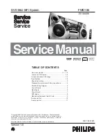
280W Mini Hi-Fi System

-/55/77/BK

Published by LX 1023 Service Audio    Subject to modification

© 

Copyright 2010 Philips Consumer Electronics B.V. Eindhoven, The Netherlands

All rights reserved. No part of this publication may be reproduced, stored in a retrieval

system or transmitted, in any form or by any means, electronic, mechanical, photocopying,

or otherwise without the prior permission of Philips.

CONTENTS

Technical specification ..................................................................1-2

Version variation ...........................................................................1-2


Service measurement setup..........................................................1-3             

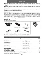
Service aids  .................................................................................1-4          

Instructions on CD playability ................................................2-1..2-2

Block diagram ................................................................................3-1

Wiring diagram ..............................................................................4-1 

Disassembly diagram............ ................................................5-1..5-2

Main board

     Circuit diagram .........................................................................6-1 

     Layout diagram ..................................................................6-2..6-3

AC board

     Circuit diagram .........................................................................7-1 

     Layout diagram ..................................................................7-2..7-3

Display board

     Circuit diagram .........................................................................8-1 

     Layout diagram ..................................................................8-2..8-3

AMP & Power Board

  Circuit diagram. ........................................................................9-1

  Layout diagram ..................................................................9-2..9-3

Tuner board

     Circuit diagram .......................................................................10-1

     Layout diagram .......................................................................10-2

CD Board

  Circuit diagram. ......................................................................11-1

  Layout diagram .............................................................. 11-2..11-3

MCU Board

  Circuit diagram. .............................................................12-1..12-2

  Layout diagram ..............................................................12-3..12-4

Exploded view diagram ...............................................................13-1

Summary of Contents for FWM452

Page 1: ...CONTENTS Technical specification 1 2 Version variation 1 2 Service measurement setup 1 3 Service aids 1 4 Instructions on CD playability 2 1 2 2 Block diagram 3 1 Wiring diagram 4 1 Disassembly diagram 5 1 5 2 Main board Circuit diagram 6 1 Layout diagram 6 2 6 3 AC board Circuit diagram 7 1 Layout diagram 7 2 7 3 Display board Circuit diagram 8 1 Layout diagram 8 2 8 3 AMP Power Board Circuit dia...

Page 2: ...ntenna MW Antenna AM Antenna USB USB host Audio Connections RCA Aux in 3 5mm stereo line in MP3 link Convenience Alarms CD Alarm USB alarm Radio Alarm Sleep timer Clock On main display Display Type LCD Karaoke MIC volume Echo control Accessories Included accessories FM MW Antenna Flat pin adaptor Batteries for remote control AC Power Cord Remote control 36 key with 2xAAA batteries Guarantee bookle...

Page 3: ...15kHz e g 7122 707 48001 LF Voltmeter e g PM2534 DUT S N and distortion meter e g Sound Technology ST1700B Frame aerial e g 7122 707 89001 Tuner AM MW LW To avoid atmospheric interference all AM measurements have to be carried out in a Faraday s cage Use a bandpass filter or at least a high pass filter with 250Hz to eliminate hum 50Hz 100Hz RF Generator e g PM5326 Ri 50 Bandpass 250Hz 15kHz e g 71...

Page 4: ...ng make sure that you are connected with the same potential as the mass of the set via a wrist wrap with resistance Keep components and tools also at this potential ESD CLASS 1 LASER PRODUCT GB Safety regulations require that the set be restored to its original condition and that parts which are identical with those specified be used Safety components are marked by the symbol Lead free ...

Page 5: ...T OK check playability N Y playability ok check playability check playability return set Customer complaint CD related problem fast lens cleaning 1 2 3 For flap loaders access to CD drive possible cleaning method 4 is recommended INSTRUCTIONS ON CD PLAYABILITY 2 1 Exchange CDM 1 4 For description see following pages ...

Page 6: ...viously caused by a scratched dirty or copy protected CD In case problems remain the customer is requested to contact the workshop directly The lens cleaning method 3 should be mentioned in the addendum sheet The final wording in national language as well as the printing is under responsibility of the Regional Service Organizations 4 LIQUID LENS CLEANING Because the material of the lens is synthet...

Page 7: ...C SENSOR 16M SDRAM 8M SERIAL FALSH SST29VF080B PICK UP MOTOR MOTOR ADC WM8782 3CDC DRIVER IC FAN8100N MUX 74LVC157 AUX TUNER SI4730 MICRO PHONE USB SD MOTOR DRIVER BA5826 IIC MUL L R IIC PCM BCK LRCK DATE PCM CD L R TUNER L R CONTROL DATA CD PCM BCK LRCK DATE AMP STK 433 870 FUNCTION IC TDA7468D 3CD LOADER FL FR ...

Page 8: ...WIRING DIAGRAM 4 1 4 1 DISPLAY BOARD KEY1 BOARD MAIN BOARD AC BOARD AMP BOARD MCU BOARD CD BOARD ...

Page 9: ... shown in the diagram below with the help of a flat head screw driver Dismantling of the CDC Module and Front Panel Remove CDC Module 4 Remove the Cover Tray CDC as indicated Sliding Out The CDC Tray Front View CDC Remove Cover Tray CDC 5 Loosen 2 screws A and 2 screws B to remove the CDC Module as indicated 6 Remove 2 screws at the bottom to separate the Front Panel Assembly from the Plate Bottom...

Page 10: ... Remove 3 screws F as indicated to loosen the Bottom Cabinet 5 Remove 2 screws G as indicated to loosen the Front Cabinet 2 Remove 4 screws D H as indicated to loosen the Main Board 3 Remove 2 screws M as indicated to loosen the USB Board 2 Remove 27 screws K L as indicated to loosen the KEY1 2 Board 1 Remove 4 screws J as indicated to loosen the AMP Board C F D E G H I J K L M ...

Page 11: ... 1 3 5 7 9 4 6 8 10 1 2 3 4 5 6 7 8 9 10 CN601 Q606 3904 R673 47K R682 47K R681 30K C638 470U 16V 1 IN 2 GND 3 OUT IC606 KA7805 R601 0R33 1W 1 C637 100N D601 1N5819 1 2 3 4 5 6 CN602 1 2 3 4 5 6 1 2 3 4 5 6 CN605 Q613 8550C Z601 4V7 Q603 3904 Q604 3904 R622 10K D603 BAS316 D604 BAS316 R635 12K GND RIGHT LEFT CN610 R638 10R C625 100U 16V C628 100N C630 100U 25V C612 100N D602 BAS316 Q614 3904 R624 ...

Page 12: ...LAYOUT DIAGRAM MAIN BOARD TOP SIDE 6 2 6 2 ...

Page 13: ...LAYOUT DIAGRAM MAIN BOARD BOTTOM SIDE 6 3 6 3 ...

Page 14: ...N4001 F807 T200mAL 250V C810 47UF R835 R834 1k R833 10R 1 6W Q801 8050D C808 10V 100U U801 LM1117 3 3V D805 1N4001 M C811 104 C807 10V 100U M C825 0 02U M C823 0 02U M C824 0 02U M C822 0 02U D824 1N4001 D822 1N4001 D823 1N4001 RL801 DC6V D821 1N4001 T802 EI28 M C827 0 02U M C804 0 02U M C826 0 02U M C803 0 02U D818 1N5402 D816 1N5402 D817 1N5402 D815 1N5402 M C833 0 02U M C834 0 02U M C832 0 02U ...

Page 15: ...PCB LAYOUT AC BOARD 7 2 7 2 ...

Page 16: ...R979 10K 14 12 10 8 6 4 15 13 11 9 7 5 3 2 1 1 2 3 4 5 6 7 8 9 10 11 12 13 14 15 CN901 1 2 3 50K x2 4 5 6 50K x2 27 26 25 24 23 22 21 20 19 18 17 16 15 14 13 12 11 10 9 8 7 6 5 4 3 2 1 LCD901 C909 47U 16V 2 4 3 5 1 CN911 2 4 3 5 1 CN914 Q909 PMBT3904 2 4 3 5 1 CN903 1 2 3 CON904 C904 1000P C903 1000P D903 5V1 C906 47U 16V C907 100N Q901 PMBT3904 D904 WHITE R953 100R C905 47U 16V R954 330R R980 10K...

Page 17: ...LAYOUT DIAGRAM DISPLAY BOARD TOP SIDE 8 2 8 2 ...

Page 18: ...LAYOUT DIAGRAM DISPLAY BOARD BOTTOM SIDE 8 3 8 3 ...

Page 19: ...V C755 100U 63V R772 47R C728 22U 50V C729 100N R758 10K C741 100N Q716 2N5551 C749 100P C751 3P C732 10U R761 1K8 C750 100P C716 120P R752 56K R751 56K C736 470N C735 470N R778 3K3 R777 3K3 1 2 CON705 C786 100U 25V R793 2R2 1 4W Q704 8050C C785 47U 50V ZD703 10V R737 470R R799 3K9 Q715 8050C R718 47K C772 0 47U 50V C777 1000U 25V C712 120P R782 47K R784 47K C721 470N C733 470N R726 27K C756 100N ...

Page 20: ...PCB LAYOUT AMP BOARD TOP SIDE 9 2 9 2 ...

Page 21: ...PCB LAYOUT AMP BOARD BOTTOM SIDE 9 3 9 3 ...

Page 22: ...CIRCUIT DIAGRAM TUNER BOARD 10 1 10 1 ...

Page 23: ...LAYOUT DIAGRAM TUNER BOARD 10 2 10 2 ...

Page 24: ...CIRCUIT DIAGRAM CD BOARD 11 1 11 1 ...

Page 25: ...LAYOUT DIAGRAM CD BOARD TOP SIDE 11 2 11 2 ...

Page 26: ...LAYOUT DIAGRAM CD BOARD BOTTOM SIDE 11 3 11 3 ...

Page 27: ...6 104 C157 104 C158 104 C159 104 C160 104 C162 104 C163 104 C164 104 C166 104 R102 100 L107 FB R145 FB600 R146 100 R147 FB600 R175 100 R176 100 R177 FB600 R178 FB600 R179 FB600 R228 100 R182 100 R184 FB600 R185 FB600 R187 FB600 R189 FB600 R190 100 R197 100 R198 100 R199 100 R109 100 R110 FB600 R111 100 R130 100 R192 100 R193 100 R194 FB600 R195 100 R196 FB600 R134 FB600 R100 100 Q102 3904 R105 2K2...

Page 28: ...8 100n EE FE TE C512 100n R523 47K R501 OR D502 IN4148 D501 IN4148 6 1 2 3 4 5 1 2 3 4 5 6 CN505 C510 100n C515 100n C522 100n 2 1 C525 47u 16v C509 100n H1 H2 1 VO1 2 VO1 3 IN1 4 RESET 5 REGB 6 REGOUT 7 MUTE 8 GND1 9 IN2 1 10 IN2 2 11 VO2 12 VO2 13 GND2 14 OPOUT 28 GND3 27 VO4 26 VO4 25 IN4 1 24 IN4 2 23 VR 22 VCC2 21 VCC1 20 IN3 2 19 IN3 1 18 VO3 17 VO3 16 RESET 15 OPIN IC502 BA5826FP C528 1 2 R...

Page 29: ...PCB LAYOUT MCU BOARD TOP SIDE 12 3 12 3 ...

Page 30: ...PCB LAYOUT MCU BOARD BOTTOM SIDE 12 4 12 4 ...

Page 31: ...SET EXPLODED VIEW 13 1 13 1 ...

Reviews: