Published by JH 563 Service PaCE
Printed in the Netherlands
Subject to modification
EN 3122 785 15020
©
Copyright 2005 Philips Consumer Electronics B.V. Eindhoven, The Netherlands.
All rights reserved. No part of this publication may be reproduced, stored in a
retrieval system or transmitted, in any form or by any means, electronic,
mechanical, photocopying, or otherwise without the prior permission of Philips.
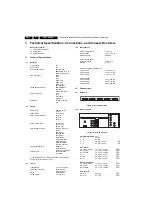
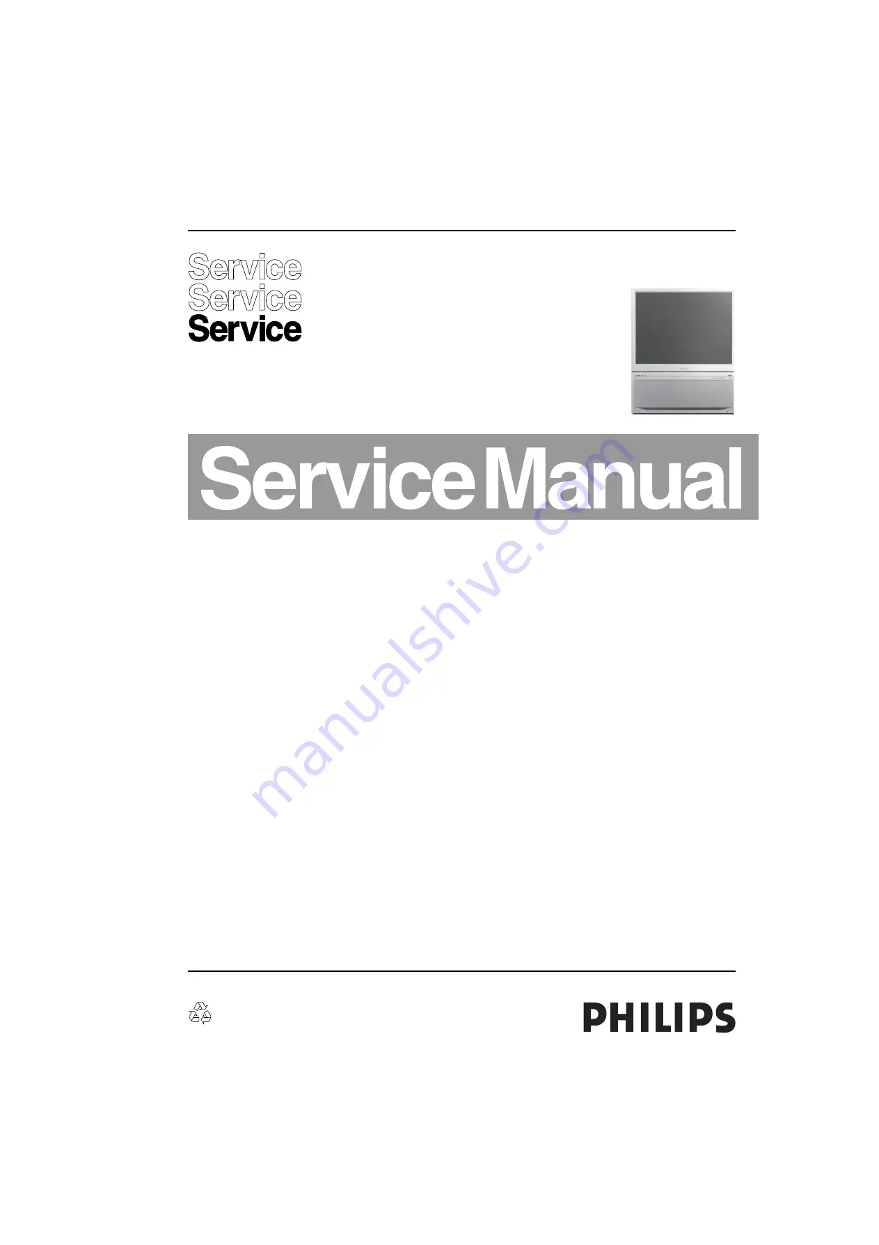
Colour Television
Chassis
DPTV565
AA
E15000_000.eps
191004
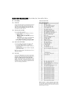
Contents
Page
Contents
Page
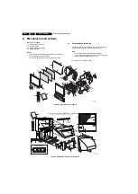
Technical Specifications, Connections, and Chassis
Overview
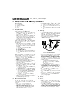
Safety Instructions, Warnings, and Notes
Service Modes, Error Codes, and Fault Finding 10
Block Diagrams, Testpoint Overviews, and
Waveforms
Wiring Diagram
Circuit Diagrams and PWB Layouts
Diagram PWB
(A1) 19
(B1) 21
(B2) 22
SSB: Feature Box (100Hz Processing)
(B3) 23
(B4) 24
(B6) 25
(B7) 26
(C1) 30
(C2) 31
(C3) 32
(C4) 33
(C5) 34
(C6) 35
(C7) 36
(C8) 37
(C9) 38
(DR1) 45
(DG1) 46
(DB1) 47
(E1) 49
(E2) 50
(E3) 51
Mapping Large Signal Panel E1-E3 (Part 1)(E4) 52
Mapping Large Signal Panel E1-E3 (Part 2)(E5) 53
(G1) 56
(H1) 58
(H2) 59
(H3) 60
(H4) 61
(J1) 64
(J2) 65
(J3) 66
Mapping HOP Panel J1 and J2 Part 1
(J4) 67
Mapping HOP Panel J1 and J2 Part 2
(J5) 68
(K1) 70
Circuit Descriptions, List of Abbreviations, and IC
Data Sheets