background image

Car Audio Video System

CED229/51/55

/

98

TABLE OF CONTENTS

Location of PCBS… … … … … … … … … …1-1
Specifications… … … … … … …… … … … …1-2
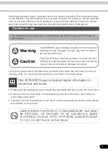
Safety Instruction, Warning & Notes ..… . 1-3

Disassembly diagram… … … … … … . … ..2-1/2

Software version check&upgrade… . … …3-1
Malfunction check chart… … … … … … . . . 3-2
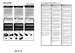
Wiring diagram… … … … … … … … … … …4-1
Main board-circuit diagram-1… … … … …5-1

Main board-circuit diagram-2… … … … …5-2

PCB layout top/bottom view … … … … … 5-3

Servo board-circuit diagram-1 … … … . … 6-1

Servo board-circuit diagram-2… … … … …6-2
Layout diagram top/bottom view… … … …6-3

SB+CB board-circuit diagram… … … . … …7-1

KEY board-circuit diagram… … … . . . … … …9-1
KEY 

board layout  diagram ....................

… . … …9-2

Exploded view-main unit ........................... 10-1

SB+CB board-layout top/bottom vie w.......7-2

LB+SD+CB board-layout diagram............8-2

LB+SD

 board-circuit diagram. . . . . … …8-1

+CB

CED229X/78

©

 Copyright 2011 Philips Consumer Electronics B.V. Eindhoven, The Netherlands

All rights reserved.  No part of this publication may be reproduced, stored in a retrieval system or 
transmitted, in any form or by any means, electronic, mechanical, photocopying, or otherwise without 
the prior permission of Philips.

Published by DB- SL 1149   BG AVM     Printed in The Netherlands 

Subject to modification

Version 1.3

CLASS 1

LASER PRODUCT

   3141 785 35593

Summary of Contents for CED229/98

Page 1: ...ircuit diagram 7 1 KEY board circuit diagram 9 1 KEY board layout diagram 9 2 Exploded view main unit 10 1 SB CB board layout top bottom view 7 2 LB SD CB board layout diagram 8 2 LB SD board circuit diagram 8 1 CB CED229X 78 Copyright 2011 Philips Consumer Electronics B V Eindhoven The Netherlands All rights reserved No part of this publication may be reproduced stored in a retrieval system or tr...

Page 2: ... 51 X 78 C M C M C M C M 98 C M C M C C C C ...

Page 3: ... 1 9kg 16V System Frequency response Signal noise ratio Total harmonic distortion Channel separation Video signal for mat Video output Disc digital audio system 20Hz 20k Hz 75dB Less than 0 3 1KHz 55dB NTSC PAL AUTO 1 0 2V Screen size Display resolution Active area Contrast ratio Brightness 3 0 inches 320x240 dots 65 52 W x36 84 H 300 200cd m 16 91 Frequency range FM Frequency range AM MW Usable s...

Page 4: ...hange 1 1 Technical Specifications For on line product support please use the following website http www p4c philips com cgi bin dcbint cpproduct_selector pl Here is product information available as well as getting started user manuals frequently asked questions and software drivers 1 2 Directions for Use You can download this information from the following websites http www philips com support ht...

Page 5: ...d voltages with and without aerial signal Measure the voltages in the power supply section both in normal operation and in stand by These values are indicated by means of the appropriate symbols 2 3 2 Schematic Notes All resistor values are in ohms and the value multiplier is often used to indicate the decimal point location e g 2K2 indicates 2 2 k Resistor values with no multiplier may be indicat...

Page 6: ... sources are expected to have a possible dangerous impact others of quite high potential are of limited current and are sometimes held in less regard Always respect voltages While some may not be dangerous in themselves they can cause unexpected reactions that are best avoided Before reaching into a powered TV set it is best to test the high voltage insulation It is easy to do and is a good servic...

Page 7: ... Frequency Interlaced Scan mode where two fields are used to form one frame Each field contains half the number of the total amount of lines The fields are written in pairs causing line flicker IR Infra Red IRQ Interrupt Request ITU 656 The ITU Radio communication Sector ITU R is a standards body subcommittee of the International Telecommunication Union relating to radio communication ITU 656 a k ...

Page 8: ...s SD Standard Definition SDA Serial Data I2 C SDA F DAta Signal on Fast I2C bus SDI Serial Digital Interface see ITU 656 SDRAM Synchronous DRAM SECAM SEequence Couleur Avec Mémoire Color system mainly used in France and East Europe Color carriers 4 406250 MHz and 4 250000 MHz SIF Sound Intermediate Frequency SMPS Switched Mode Power Supply SoC System on Chip SOG Sync On Green SOPS Self Oscillating...

Page 9: ...iver 15 Loosen and take out the six bolts with a screwdriver 12 loosen and take out the bolt with a screw driver 13 loosen and take out the bolt with a screw driver 14 P carefully ull out the two pieces of connection pegs Disassembly Diagram 2 2 2 2 ...

Page 10: ...ick 6 When software upgrade complete the device will power off automatically 1 Copy the file ROM BIN into USB stick note to delete the file MCU BIN 2 Power on the device and plug the USB stick into USB socket After the device read the content in the USB the LCD will show a upgrade menu and enter into the upgrading status 3 The LCD will appear a number changed from 20 to 0 and when arrived the numb...

Page 11: ...hich in Main board NO NO NO Change main Check tuner circuit and its conjoint part is good or bad NO NO NO NO NO NO SD no read Change servo Whether connect to SD Check the socket of SD SD USB no read Change servo Whether connect to USB Check the socket of USB SD ...

Page 12: ...4 1 4 1 WIRING DIAGRAM ...

Page 13: ...5 1 5 1 MAIN BOARD CIRCUIT DIAGRAM 1 ...

Page 14: ...5 2 5 2 MAIN BOARD CIRCUIT DIAGRAM 2 ...

Page 15: ...5 3 5 3 MAIN BOARD PCB LAYOUT TOP BOTTOM VIEW ...

Page 16: ...6 1 6 1 SERVO BOARD CIRCUIT DIAGRAM 1 ...

Page 17: ...6 2 6 2 SERVO BOARD CIRCUIT DIAGRAM 2 ...

Page 18: ...6 3 6 3 SERVO DIAGRAM BOARD LAYOUT TOP BOTTOM VIEW ...

Page 19: ...7 1 7 1 SB CB BOARD CIRCUIT DIAGRAM ...

Page 20: ...7 2 7 2 SB CB BOARD PCB LAYOUT TOP BOTTOM VIEW ...

Page 21: ...8 1 8 1 LB SD CB BOARD CIRCUIT DIAGRAM ...

Page 22: ...LB SD PCB CB BOARD LAYOUT TOP BOTTOM VIEW 8 2 8 2 ...

Page 23: ...9 1 9 1 KEY BOARD CIRCUIT DIAGRAM ...

Page 24: ...9 2 9 2 KEY BOARD LAYOUT DIAGRAM TOP VIEW BOTTOM ...

Page 25: ...Remark Pos No 14 Key Board Ass y cannot be ordered seperately and must be ordered with whole Front Panel Ass y Pos No 101 ...

Reviews: