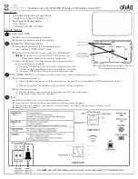


CD Sound Machine
AZ6188
©
3140 785 32800
Published by LX 0432 Service Audio Printed in The Netherlands Subject to modification
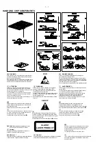
CLASS 1
LASER PRODUCT
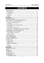
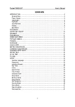
TABLE OF CONTENTS
©
Copyright 2004 Philips Consumer Electronics B.V. Eindhoven, The Netherlands
All rights reserved. No part of this publication may be reproduced, stored in a retrieval
system or transmitted, in any form or by any means, electronic, mechanical, photocopying,
or otherwise without the prior permission of Philips.
Handling Chip Components and Safety ..........................1 - 1
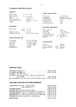
Technical Specification & Service tools ...........................2 - 1
Service Measurement......................................................2 - 2
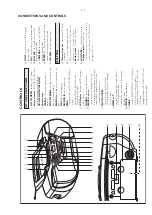
Connections and controls ................................................3 - 1
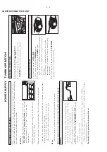
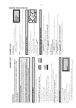
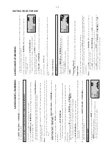
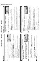
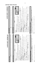
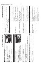
Instructions for use ..............................................3 - 2 to 3 - 8
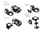
Disassembly Diagram......................................................4 - 1
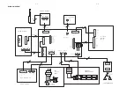
Block Diagram .................................................................5 - 1
Wiring Diagram ................................................................5 - 2
Front Board
Circuit diagram ........................................................6 - 1
layout diagram........................................................6 - 2
Tuner Board
circuit diagram .........................................................7 - 1
layout diagram.........................................................7 - 2
Recorder Board
circuit diagram .........................................................8 - 1
layout diagram.........................................................8 - 2
Combi Boad
circuit diagram .............................................9 - 1 to 9 - 6
layout diagram............................................9 - 7 to 9 - 8
Exploded view ..............................................................10 - 1
Mechanical partslist .......................................................10 - 2
Electrical partslist...........................................................10 - 2
all versions
version 1.0