background image

Published by MW 0765 BG CD Customer Service

Printed in the Netherlands

Subject to modification

EN 3122 785 16392

©

Copyright 2007 Philips Consumer Electronics B.V. Eindhoven, The Netherlands.

All rights reserved. No part of this publication may be reproduced, stored in a 
retrieval system or transmitted, in any form or by any means, electronic, 
mechanical, photocopying, or otherwise without the prior permission of Philips.
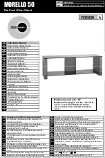
Colour Television

Module

LGE PDP 2K6

 PDP42X3*

Contents

Page

1.

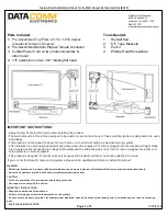
Technical Specifications, Connections, and Chassis 
Overview

2

2.

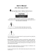
Safety Instructions, Warnings, and Notes

5

3.

Directions for Use

6

4.

Mechanical Instructions

7

5.

Service Modes, Error Codes, and Fault Finding 12

6.

Block Diagrams, Test Point Overviews, and 
Waveforms

25

7.

Circuit Diagrams and PWB Layouts

25

8.

Alignments

26

9.

Circuit Descriptions, Abbreviation List, and IC Data 
Sheets

29

10. Spare Parts List

34

11. Revision List

34

Summary of Contents for 43FDX01B

Page 1: ...l photocopying or otherwise without the prior permission of Philips Colour Television Module LGE PDP 2K6 PDP42X3 Contents Page 1 Technical Specifications Connections and Chassis Overview 2 2 Safety Instructions Warnings and Notes 5 3 Directions for Use 6 4 Mechanical Instructions 7 5 Service Modes Error Codes and Fault Finding 12 6 Block Diagrams Test Point Overviews and Waveforms 25 7 Circuit Dia...

Page 2: ...5 Manufacture date Year Month 6 The place of origin 7 Model suffix Figure 1 3 Voltage label on rear side of module Model Name PDP42X3 Number Of Pixels H x V 1024 3 x 768 Pixel Pitch H x V µm 900 x 676 Cell Pitch H x V µm 300 x 676 base Green Cell Display Area H x V mm 921 6 x 519 2 0 5 Outline Dimension H x V x D mm 1005 x 597 x 61 2 1 Colour Arrangement RGB closed type Number Of Colours R x G x B...

Page 3: ...E PDP 2K6 1 Figure 1 4 Part number printing on board Figure 1 5 Part number label on board Figure 1 6 TCP serial number on TCP PCB PART NO G_16390_008 eps 040806 G_16390_005 eps 020806 BOARD SERIAL NR BOARD NAME BOARD ASSY PART NR G_16390_007 eps 030806 TCP SERIAL NO ...

Page 4: ...ions Connections and Chassis Overview EN 4 LGE PDP 2K6 1 1 1 3 Chassis Overview Figure 1 7 PWB location G_16391_002 eps 290607 Control Board Z Sus Board Y Sus Board X Right Board X Left Board Y Driver Board PSU 3501Q00203B ...

Page 5: ...oid conductive materials 13 If inserting components or circuit boards in order to repair be sure to fix a lead line to the connector before soldering 14 If inserting high power resistors metal oxide film resistor or metal film resistor in order to repair insert it 10 mm away from a board 15 During repairs high voltage or high temperature components must be put away from a lead line 16 This is a co...

Page 6: ...Directions for Use EN 6 LGE PDP 2K6 3 3 Directions for Use Not applicable ...

Page 7: ...ustain Board 4 2 4 Y Driver Board 4 2 5 Z Sustain board 4 2 6 X board 4 1 Mechanical Overviews Figure 4 1 Cable dressing Table 4 1 Cable function G_16391_004 eps 020707 8 4 1 2 3 6 5 7 Cable No Function 1 Drive signal for Y waveform 2 3 RGB data to be transferred to panel 4 5 5V and Va supply for X boards Left and Right 6 Drive signal for Z waveform 7 8 Va Vs and 5 V supply for PDP operation ...

Page 8: ...Mechanical Instructions EN 8 LGE PDP 2K6 4 Figure 4 2 Label location on PWB s Figure 4 3 Label indication G_16390_014 eps 070806 G_16390_013 eps 070806 ...

Page 9: ...ectronics 6 TUV Approval Mark 7 Safety Approval Mark 8 Safety Approval No 3 Voltage Label Model Name Operational Voltage 2 5 7 cm G_16390_020 eps 020707 4 Serial No for Frame Ass y 1 Serial No of Frame Ass y Serial No of Frame Ass y for Philips are 3315Q E037B 3315Q E037C and 3315Q E037F 5 Manufacture Serial No Label of Module 1 Model Name Model Names for Philips are PDP42X3A062 PDP42V7A012 PDP42V...

Page 10: ...ugging connectors 3 Do not touch the heatsink Figure 4 8 Y SUS board removal 4 2 4 Y Driver Board 1 Remove the Y SUS board 1 as described previously 2 Remove the fixation screws 2 3 Separate the TCP s 3 Figure 4 9 Y driver board removal Figure 4 10 TCP Separation G_16390_031 eps 010906 1 2 2 2 2 2 2 2 1 1 3 3 G_16390_032 eps 010906 3 2 2 1 2 F_15590_050 eps 040705 ...

Page 11: ... Pull FPC as shown by arrow Figure 4 11 Z SUS board removal Figure 4 12 FPC removal 4 2 6 X board 1 Unplug the power cable 2 Unplug the signal cable 3 Remove the heatsink 4 Separate the TCP s 1 5 Remove the fixation screws 2 Figure 4 13 X board removal 1 2 Figure 4 14 X board removal 2 2 Figure 4 15 TCP Separation G_16390_033 eps 0108069 1 1 2 2 2 2 3 3 2 F_15590_052 eps 040705 Signal cables G_163...

Page 12: ...display Bar defect appeared Please follow Bar defect trouble shooting way later on in this chapter Line defect Please follow the Line defect trouble shooting way later on in this chapter Mis discharge on screen Please follow the Mis discharge trouble shooting way later on in this chapter G_16390_018 eps 300806 Y Y Y Y N N N N Y Y Trouble Shooting Horizontal defect Vertical defect Mis discharge on ...

Page 13: ...il Figure 5 3 Control Y SUS board Figure 5 4 Control Z SUS board Figure 5 5 Control X board Figure 5 6 Signal input LVDS Exhaust Tip Check the Exhaust Tip for cracks with the naked eye to check the vacuum state If there is a problem replace the PDP module by a new one In case of vacuum breakdown the module makes a shaking noise because of inside gas ventilation There may be a small crack which can...

Page 14: ...nction protects the boards when a short occurs on circuits of the PDP module or when a power problem occurs If there is no power even after replacing the PSU find out where the short occurred In case of a PSU protection the red LED will be ON and an error code will be displayed via the green blinking LED see also paragraph Detailed PSU Trouble Shooting further on In case of a PSU protection discon...

Page 15: ...So if there is a bar defect on screen it may be a Control board problem Figure 5 13 Control board address flow 5 1 3 Line Defect Vertical In case of one line open or shorted check for dirt foreign substances in TCP connector First try to remove the dirt with compressed air If after this the same line appears again replace the panel Line Open or Short This phenomenon is due to a TCP IC internal sho...

Page 16: ...ctors and YSUS YDRV first Figure 5 16 Check FPC connectors Figure 5 17 Check drive connectors Scan IC Check Check the diode value of the right side part of the output pin Figure 5 18 Scan IC output diode check 5 1 5 Line Defect Horizontal FPC Check In case of one or more horizontal lines this is probably due to FPC or panel inside the Control board Y board is just normal Figure 5 19 Open FPC elect...

Page 17: ...st diode values are over 0 4 OK Reverse direction Measure between GND and Sus out Sus out and Vs When all test diode values are infinite OK Figure 5 22 IPM check 5 2 Detailed Module Check 5 2 1 No Display The Screen Does Not Display a Picture 1 Check whether on the CTRL board LED D12 D13 D14 is turned ON or not 2 Check the power and signal cable of the CTRL board 3 Check if the X Y and Z boards ar...

Page 18: ...Service Modes Error Codes and Fault Finding EN 18 LGE PDP 2K6 5 Figure 5 23 Output waveforms on X Y and Z boards G_16390_043 eps 300806 ...

Page 19: ...n be shown Figure 5 25 Screen display Vertical parts missing How to examine the Data TCP IC Connect 1 Va Power to the minus and 2 GND to the plus of an ohmmeter and then examine the diode in forward or reverse direction Examine with the naked eye traces of blown ICs 3 or other parts Figure 5 26 Data TCP IC examination Unusual Pattern on Display 1 In case of generation of an unusual pattern of the ...

Page 20: ...board operation is not complete 2 Check the power cord of Z board 3 Check the connector of Z board and CTRL board 4 Replace the CTRL board or Z board Partially Other Colour on Full White Screen or Partially Mis Discharge on Full Black Screen 1 Check the Y board waveform see below 2 Measure the output wave with an oscilloscope 200 MHz and compare the waveform with the waveform in the figure below A...

Page 21: ...defective When the Set_down FET Pass_Top FET 1st 3rd 4th 5th FFT of HS2 is damaged mis discharge of the entire screen is generated Test Point GND Waveform Y DRV board Wave format as shown in the figure below Figure 5 37 Set_down FET defective SCAN IC Y DRV board IC1 10 1 In case of the SCAN IC is damaged one horizontal line may be open on the screen Test Point ICT output GND on the Y DRV board Wav...

Page 22: ...ow no image on the corresponding part or mis discharge In most cases you can see a burn mark on the IC Test Point Output TP of GND TCP Wave format No output wave Figure 5 41 COF IC output defective Figure 5 42 TCP normal output Crystal CTRL board X1 1 When a crystal is damaged the screen is not shown Test Point 3 pin of GND Crystal CTRL board X1 Wave format Output wave is not generated 2 In case o...

Page 23: ...e Modes Error Codes and Fault Finding EN 23 LGE PDP 2K6 5 Figure 5 43 Crystal normal output Figure 5 44 Crystal defective output ZUZ F_15590_036 eps 040705 XU Y v G G G G G G p G G G SG F_15590_035 eps 060605 ...

Page 24: ...acklight No picture Picture too bright Scratches LCD only acc Pixel criteria sheet V4 0 Only partial picture Unstable picture Flickering flashing picture Lines across down image Inactive row s Inactive column s Missing colour s Light leakage Other PANEL REPAIR Pixel Defect s Symptoms Out of warranty Dark dots Bright dots Qty of dots Mark Defect s These symptoms are not claimable Following defect s...

Page 25: ... Applied Voltage level is specified at the time when Full White pattern is displayed on the panel Color PDP 1024 X 768 pixels Address Driver r e v i r D n a c S r e v i r d n i a t s u s n o m m o C Vcc 5V Display data Driver timing Memory Controller Driver Timing Controller Input Interface Controller Va 60 1V Vs 175V 190V Controller External Power RA RA RB RD RD RB RC RC RE RE RCLK RCLK LVDS inpu...

Page 26: ... within 1 for Vs and Va within 3 for 5V 8 2 2 Connection Diagram and Set Up 1 For the connection diagram of the measuring instrument refer to Fig Measuring equipment connection diagram 2 Set up the initial voltage Vcc 5 V Va 60 V Vs 180 V Note that the initial set up voltage can be changed according to the module s characteristics the values on the voltage label 3 Environmental conditions temperat...

Page 27: ... Vy voltage across R36 or on the Vy test point on the DC converter on the Y SUS board see Figure Y SUS Alignment 2 Adjust Vy to the value indicated on the voltage sticker with potentiometer VRy on the Y SUS board Y SUS Set up Voltage Waveform Adjustment Now connect the oscilloscope between the Waveform test point on the Y Driver board and GND see Figure Y SUS Alignment Trigger with Vs DA on the Co...

Page 28: ...Test Patterns The CTRL board is capable of generating its own video test patterns To generate the test patterns do as follows Disconnect the mains cord Disconnect the SSB of the TV set by removing the cables of connectors 1M03 and 1M46 on the PSU Reconnect the mains cord Connect pins 1 2 or pins 3 4 of Connector P1 on the Control Board see Figure below to each other Now the internal test patterns ...

Page 29: ...rrier Package 9 12 IPM Intelligent Power Modules 9 13 Abbreviation List 9 14 IC Data Sheets 9 1 Introduction The 42X3 panel is LGE s HD successor for the year 2007 of the 42V7 panel 9 2 Power Supply Unit PSU 9 2 1 Purpose To convert an input voltage of 100 240 Volt AC to voltages that the different boards and the panel need Output voltages Vcc 5 V Vs 180 200 V and Va 60 65 V all DC The PSU switche...

Page 30: ...power supply is switched ON OFF above sequence should be observed strictly ත Transition section Transition section is needed to drive PDP as a initial and set up period At this period Brightness is low and there is no gray ත If DISPEN is low picture is changed to BLACK pattern Signal is operated by synchronized vertical signal ත The panel will not malfunction if DISPEN is high at start up Min 2 fr...

Page 31: ...fference is 0 V between GND and Vpp of the DRIVER IC during the SUSTAIN period Generates a potential difference between GND and Vpp only during the SCAN period Figure 9 6 Y Drive board 9 7 Z Sustain Board 9 7 1 Purpose To make the SUSTAIN and ERASE pulses that generate SUSTAIN discharge in the panel by receiving LOGIC signal from CONTROL board This waveform is then supplied to the panel through FP...

Page 32: ... sided these have a pattern on it For Z board there is no pattern single sided and Beta type all of copper surface Figure 9 10 Flexible Printed Circuit 9 10 FFC Flat Flexible Cable 9 10 1 Purpose For connecting LOGIC signals between boards There are two types 0 5 mm pitch 50 pin type 1 0 mm pitch 30 pin type Figure 9 11 Flat Flexible Cable 9 11 TCP Tape Carrier Package 9 11 1 Purpose To supply a 6...

Page 33: ...l Film CTRL Control board DC Direct Current FET Field Effect Transistor FPC Flexible Printed Circuit I O Input Output IC Integrated Circuit IPM Intelligent Power Module LED Light Emitting Diode LGE Lucky Goldstar Electronics supplier MCM Multi Chip Module PCB Printed Circuit Board same as PWB PDP Plasma Display Panel PFC Power Factor Corrector circuit PSU Power Supply Unit PWB Printed Wiring Board...

Page 34: ...xxx xxxx 0 First release Manual xxxx xxx xxxx 1 References in text and graphics to PSU model 3501Q00201A not used in this PDP model changed to references to PSU model 3501Q00203B Corrections in texts referring to the PSU Y SUS and Z SUS boards Manual xxxx xxx xxxx 2 Text on how to generate Internal Test Patterns added to Chapter 8 Alignments Minor text corrections added ...

Reviews: