background image

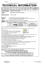
Published by EL 0564 TV Service

Printed in The Netherlands

Subject to modification

EN 3122 785 15460

©

Copyright 2005 Philips Consumer Electronics B.V. Eindhoven, The Netherlands.

All rights reserved. No part of this publication may be reproduced, stored in a 
retrieval system or transmitted, in any form or by any means, electronic, 
mechanical, photocopying, or otherwise without the prior permission of Philips.

Colour television

Chassis

FTP2.4E

AA

Service Manual FHP plasma panels: 3122 785 14580

Service Manual SDI plasma panels: 3122 785 14990

E_14650_000.eps

160604

Contents

Page

Contents

Page

1.

Technical Specifications, Connections, and Chassis 
Overview

2

2.

Safety Instructions, Warnings, and Notes

5

3.

Directions for Use

6

4.

Mechanical Instructions

7

5.

Service Modes, Error Codes, and Fault Finding 12

6.

Block Diagrams, Testpoint Overviews, and 
Waveforms

Wiring Diagram 42 Inch FHP Step

23

Wiring Diagram 50 Inch SDI Step

24

Block Diagram Supply 42 Inch FHP

25

Block Diagram Video

26

Block Diagram Audio & Control

27

I2C IC’s overview

28

Supply Lines Overview FHP

29

Supply Lines Overview SDI

30

7.

Circuit Diagrams and PWB Layouts

Diagram PWB

PDP Supply Panel: Filter Standby

(A2) 31

36-41

PDP Supply Panel: Protection

(A3) 32

36-41

PDP Supply Panel: Pre-Conditioner

(A5) 33

36-41

PDP Supply Panel: LLC Supply

(A6) 34

36-41

PDP Supply Panel: AUX Supply

(A7) 35

36-41

Ambi Light

(AL) 42

43

SSB: IF, I/O Video Processing

(B2) 44

78-89

SSB: PICNIC

(B3A) 45

78-89

SSB: (FEM) Falconic Embedded Memory (B3B) 46

78-89

SSB: Eagle

(B3C) 47

78-89

SSB: Columbus

(B3D) 48

78-89

SSB: FBX Supply

(B3E) 49

78-89

SSB: HOP

(B4) 50

78-89

SSB: OTC-Flash

(B5A) 51

78-89

SSB: Backlight Control

(B5B) 52

78-89

SSB: OTC-Flash

(B5C) 52

78-89

SSB: Audio Demodulator

(B6A) 53

78-89

SSB: Dolby Digital Decoder

(B6B) 54

78-89

SSB: Dolby Pro Logic Processor

(B6C) 55

78-89

SSB: Audio Delay

(B6D) 56

78-89

SSB: DC/DC Convertor

(B12) 57

78-89

SSB: Main Tuner

(B13A) 58

78-89

SSB: Sub Tuner

(B13B) 59

78-89

SSB: DC/DC Converter

(B13C) 60

78-89

SSB: I/O1: MMC

(B14A) 61

78-89

SSB: I/O2: Connections

(B14B) 62

78-89

SSB: I/O3: Switch

(B14C) 63

78-89

SSB: I/O4: Audio

(B14D) 64

78-89

SSB: I/O: 5

(B14E) 65

78-89

SSB: I/O6: Digital Input

(B14F) 66

78-89

SSB: I/O: 7

(B14G) 67

78-89

SSB: PIP HIP

(B15A) 68

78-89

SSB: PIP Switch

(B15B) 69

78-89

SSB: PIP Muppet

(B15C) 70

78-89

SSB: HDI A/D Converter

(B19A) 71

78-89

SSB: EPLD Control

(B19B) 72

78-89

SSB: EPLD OSD

(B19C) 73

78-89

SSB: EPLD I/O

(B19D) 74

78-89

SSB: Backlight Control

(B19E) 75

78-89

SSB: Screen Interface

(B20) 76

78-89

SSB: Connection

(B21) 77

78-89

PDP Audio Amplifier

(C) 90

91

Side I/O Panel

(D) 92

93

Top Control Panel

(E) 94

95

SCART 3 Panel

(H) 96

97

LED and Switch Panel

(J) 98

99

8.

Alignments

101

9.

Circuit Descriptions, Abbreviation List, and IC Data 
Sheets

107

10. Spare Parts List

110

11. Revision List

123

Summary of Contents for 3122 785 14580

Page 1: ...er A5 33 36 41 PDP Supply Panel LLC Supply A6 34 36 41 PDP Supply Panel AUX Supply A7 35 36 41 Ambi Light AL 42 43 SSB IF I O Video Processing B2 44 78 89 SSB PICNIC B3A 45 78 89 SSB FEM Falconic Embedded Memory B3B 46 78 89 SSB Eagle B3C 47 78 89 SSB Columbus B3D 48 78 89 SSB FBX Supply B3E 49 78 89 SSB HOP B4 50 78 89 SSB OTC Flash B5A 51 78 89 SSB Backlight Control B5B 52 78 89 SSB OTC Flash B5...

Page 2: ... 5 5 5 74 NICAM B G 5 5 5 85 NICAM D K 5 5 5 85 NICAM I 6 0 6 52 Maximum power WRMS 2 x 15 1 1 3 Miscellaneous Power supply Mains voltage VAC 220 240 Mains frequency Hz 50 60 Ambient conditions Temperature range C 5 to 40 Maximum humidity 90 R H Power consumption Normal operation W 42 257 50 375 Stand by W 2 Dimensions WxHxD cm 42 111x78x10 50 128x88x10 Weight kg 42 42 50 58 1 2 Connections Note T...

Page 3: ...o Gnd H 18 Ground FBL Gnd H 19 Video CVBS 1 VPP 75 ohm k 20 Video CVBS 1 VPP 75 ohm j 21 Shield Gnd H Cinch Sub woofer Out Centre In Bu Centre 0 5 VRMS 10 kohm jq Bk Sub woofer 0 5 VRMS 10 kohm kq Cinch Audio Out Rd Audio R 0 5 VRMS 10 kohm kq Wh Audio L 0 5 VRMS 10 kohm kq Cinch DVI Audio In Rd Audio R 0 5 VRMS 10 kohm jq Wh Audio L 0 5 VRMS 10 kohm jq DVI I Digital Analogue Video In Figure 1 4 D...

Page 4: ...1 1 3 Chassis Overview Figure 1 5 PWB location photo from 42 FHP model D SIDE I O PANEL C PDP AUDIO PANEL A PDP SUPPLY PANEL ONLY FOR FHP SETS H SCART 3 PANEL J LED PANEL E TOP CONTROL PANEL AL AMBI LIGHT PANE AL AMBI LIGHT PANEL L B SMALL SIGNAL BOARD F_15460_076 eps 130405 ...

Page 5: ...Hz R 1 kHz unless stated otherwise and picture carrier at 475 25 MHz for PAL or 61 25 MHz for NTSC channel 3 Where necessary measure the waveforms and voltages with D and without E aerial signal Measure the voltages in the power supply section both in normal operation G and in stand by F These values are indicated by means of the appropriate symbols The semiconductors indicated in the circuit diag...

Page 6: ...th leaded soldering tin parts is possible but PHILIPS recommends strongly to avoid mixed regimes If this cannot be avoided carefully clear the solder joint from old tin and re solder with new tin Use only original spare parts listed in the Service Manuals Not listed standard material commodities has to be purchased at external companies Special information for lead free BGA ICs these ICs will be d...

Page 7: ...ities created The buffers from the packaging Foam bars created for Service Aluminium service stands created for Service 4 2 1 Foam Bars Figure 4 2 Foam bars The foam bars order code 3122 785 90580 for two pieces can be used for all types and sizes of Flat TVs By laying the TV face down on the ESD protective foam bars a stable situation is created to perform measurements and alignments By placing a...

Page 8: ...move all T10 tapping screws 2 around the edges of the rear cover 3 Lift the rear cover from the TV 4 3 3 Ambient Light Panel s Figure 4 6 Ambient light inverter left side Figure 4 7 Ambient light inverter right side Later models are equipped with two Ambient Light Inverter panels For the earlier models with one panel reference is made to the FTP2 2x Service Manual for the correct mechanical instru...

Page 9: ...ounting screws 2 After removing the cover plate you can access the speakers 3 Be sure that the foam that makes the unit airtight is not damaged 4 3 11 SSB Figure 4 9 SSB top shielding Figure 4 10 Connector plate Figure 4 11 SSB removal 1 Remove the LVDS locking bracket 1 2 Remove all fixing screws 2 3 Disconnect the grounding wire from the mains filter 2a 4 Shift and lift the shielding at the top ...

Page 10: ...Next step is to unplug the following connectors see also Wiring Diagram in chapter 6 Mains plug on PSU Audio panel supply plug on PSU LVDS plug on SSB first remove the fixation clamp Ambilight supply plug on PSU SSB supply plugs on PSU Side Top Control plug on LED panel Side I O plug on LED panel SSB grounding wire Loosen all necessary cables from their clamps 6 Lift the plastic frame together wit...

Page 11: ...ion see figure Cable dressing EMC Shielding foam is intact LVDS connector SSB is secured with plastic clamp All grounding wires are re connected Between metal speaker grid and frame near the LED panel Between the Mains Filter and the SSB Top Shielding see figure SSB Top shielding item 2a Between the SSB Top Shielding and the PSU see figure SSB Top shielding item 2b Figure 4 15 Grounding wire of me...

Page 12: ... at 50 except volume at 25 All service unfriendly modes if present are disabled like Sleep timer Child parental lock Blue mute Automatic volume limiter AVL Auto switch off when no video signal was received for 10 minutes Skip blank of non favourite pre sets Smart modes Auto store of personal presets Auto user menu time out How to activate SDM Use one of the following methods Use the standard RC tr...

Page 13: ...g This will give the Philips Service department an extra possibility for diagnosis e g when Development asks for this Initialise the NVM same as in the past however now it happens conscious Store All options and alignments are stored when pressing the OK button Functional Test All devices are tested via the OK button Eventual errors are displayed in the error buffer The error buffer is not erased ...

Page 14: ...e value can vary from 0 brightness is minimum to 100 brightness is maximum Brightness values can be changed via the CURSOR LEFT and CURSOR RIGHT keys on the RC transmitter after pressing the MENU button and selecting PICTURE and BRIGHTNESS Contrast Gives the last status of the contrast as set by the customer The value can vary from 0 contrast is minimum to 100 contrast is maximum Contrast values c...

Page 15: ...n one value is shown Program Category Indicates the theme of the selected transmitter MOVIES NEWS SHOWS SPORTS CHILDREN MUSIC CULTURE or SERIES TV Ratings Lock Only applicable for US Movie Ratings Lock Only applicable for US V Chip TV Status Only applicable for US CUSTOMER SERVICE MENU 5 V Chip Movie Status Only applicable for US Options 1 Gives the option codes of option group 1 as set in SAM Ser...

Page 16: ...e ComPair interface box and the TV communicate via a bi directional service cable via the service connector The ComPair fault finding program is able to determine the problem of the defective television ComPair can gather diagnostic information in two ways Automatic by communication with the television ComPair can automatically read out the contents of the entire error buffer Diagnosis is done on ...

Page 17: ...een info Start TXT acquisition and time extraction Reset Audio low and Initialize MSP Screen type 400msec t 200msec Trapped Startup 2 5V and 8V is switched on Put Stand by line LOW CPU GO becomes HIGH Keep sound amplifiers muted with sound enable high 8V and 5V get their nominal level detected by the OTC Read rest of NVM information activate protection algorithms for 8V and 5V and I C start I C pr...

Page 18: ...ure that old error codes are no longer present Before clearing the buffer write down the content as this history can give you significant information If possible check the entire contents of the error buffer In some situations an error code is only the result of another error code and not the actual cause e g a fault in the protection detection circuitry can also lead to a protection There are var...

Page 19: ... to protection and it is possible that you have to wait 30 seconds before the blinking LED procedure starts 5 7 1 Introduction This chassis has only one microprocessor OTC which remains active during Stand by This because power of the microprocessor and the attached memory chip set is coming from the 3V3 supply which is derived from the 5V Stand by circuitry Therefore in both Power on as in Stand ...

Page 20: ...le that you have an Audio DC Protection because of an interruption in one or both speakers the DC voltage that is still on the circuit can not disappear through the speakers 5 8 Repair tips 5 8 1 Power Supply Unit for Fujitsu FHP plasma displays Below a troubleshoot sequence for the FHP power supply is given so this is not valid for the SDI power supply this is explained further on Stand by Supply...

Page 21: ...ommand mute 062500 ok When you have found the error check the circuitry related to the supply voltage and I2 C communication or the circuitry that triggers the protection No picture LED blinking with code 6 6 6 or 18 18 18 No communication on slow I2C or fast I2C bus As processor cannot communicate with one of the 2 buses the Stand by LED spontaneously starts blinking 6 6 6 etc or 18 18 18 etc If ...

Page 22: ...he software downloading procedure can be reached through a gap in the back cover or the SSB shielding The switch can be operated with a toothpick or something like that Make sure that you do not damage the PWB with sharp objects You can find more information on how this procedure works in the ComPair file It is possible that not all sets are equipped with the hardware needed to make software upgra...

Page 23: ...12P 6P N C 9P N C 31P 3P 7P 11P 10P 12P N C 11P 5P 5P 11P 11P 11P 20P 4P 11P 7P 6P N C LS LEFT AUDIO AMPLIFIER A 0352 7P 7P 1M10 1M03 10P 0311 0306 9P 6P 1M02 7P 1M52 9P 1735 3P DELTA MODULE 8345 8220 WIRING 42 FHP 8736 8735 8303 8302 8352 8346 0323 10P TO DISPLAY TO DISPLAY 8199 H Tuner Splitter 1T01 2nd Tuner 1T02 8336 With 3th SCART 8336 8337 With 3th SCART LVDS CONNECTOR DISPLAY Without 3th SC...

Page 24: ...P 11P 11P 6P N C LS LEFT AUDIO AMPLIFIER 1M02 7P 1M52 9P 1736 3P 1735 3P DELTA MODULE 8345 8220 SUB PSU PSU PDP 2P3 4P 7P 11P 5P 10P LS RIGHT WIRING 50 SDI 8337 With 3th SCART 8336 With 3th SCART 8352 8736 8735 8346 8302 8303 OPTIONAL OPTIONAL Tuner splitter 1T01 2nd Tuner 1T02 H 8336 LVDS CONNECTOR DISPLAY CN9007 CN9004 CN9006 CN9005 Without 3th SCART AMBIENT LIGHT 2 AL 4P 1M49 4P 1M08 3P 1M48 4P...

Page 25: ...54 3390 5V_STBY_SW 3396 3305 3303 3302 3316 3397 5V_STBY_SW 3364 5V_STBY_SW 12V_OVP 3389 6347 6362 3361 SUPPLY ON 6364 6340 6341 7389 7351 7352 3353 3344 3349 3202 VCC_GO 3224 FAN CONTROL 3225 8V6 DETECTION CIRCUIT 8V6 UNDER VOLTAGE PROT 7362 VCC_GO 2 5Vref VA VA 30V VS VS_UNSW 70 90V VB BIAS 12V 3363 7366 2 6378 5 7 7326 7327 6 3360 9V_STBY_SW 3388 3358 3332 3338 3333 3321 5225 7200 BSN304 7217 P...

Page 26: ...2 11 11 14 17 20 23 26 27 28 29 DISPLAY MF 1 17 U VOUT 0 9 Y OUT 0 9 G OSD 0 5 R OSD 0 5 BL OSD 0 5 B OSD 0 5 UVG 0 7 YG 0 7 YF 0 7 UVF 0 7 1 2 3 4 5 6 7 8 9 10 11 12 13 14 15 CLK OSD 10 11 7L01 AD9883AKST 2 9 70 77 12 19 V 2FH Y 2FH U 2FH 7001 SAA5801H 3064 1 3858 77 R TXT 2FHR GFX R OSD 3064 2 3859 78 G TXT 2FHG GFX G OSD 3064 3 3860 79 B TXT 2FHB GFX B OSD 3064 4 3861 80 FB TXT 2FHFB GFX BL OSD...

Page 27: ...1 3074 4 3097 SAM SDM 95 SOUND ENABLE 94 RESET AUDIO 117 116 SEL_IN_2 91 SDA 92 5 6 SCL 16 17 1001 6Mhz SEL_IN_1 7006 LH28F320BJE 7007 MSM51V18165F 7012 M29W400BT 7018 7019 103 PWW BLACKLIGHT B5B ADDRESS DATA CONTROL MENU CHANNEL CHANNEL VOLUME VOLUME 1M36 RP RESET FLASH RAM 7002 7004 7013 7014 DRAM TXT 16Mbit PROGRAM FLASH RAM SET SW 32Mbit 7011 MC24C32 EEPROM NVM 4kByte RP 1 7005 LF33AB OCTAL BU...

Page 28: ...2 86 3064 1 85 3092 5V2_CON 3088 DVI INPUT CONNECTOR 9T10 5 4 9T09 1T02 UV1318S SUB TUNER 9T08 5 4 9T07 1T01 UV1318ST MAIN TUNER ERR 13 RES VCC 7T50 P82B96TD 3L06 3L03 57 56 7L01 AD9883AKST A D CONVERTER 3E18 3E19 57 56 7E23 AD9883AKST A D CONVERTER 3V38 3V37 TO DISPLAY LED SWITCH PANEL ITV 3T05 3T06 3Y09 3Y40 3V3 IO 5V I2C BUFFER RES 3Z51 3Z50 ADDRESS 34 41 7760 SAA4998H V1 FEM ERR 26 ERR 6 DATA ...

Page 29: ...5EB 2V5EA 3V3EA 3V3EB 5V2Pr 3V3EC 3V3ED 2V5ED 2V5EC 1V5EA 1V5EB 2V5EB 2V5EA 3V3EA 3V3EB 5V2Pr 3V3EC 3V3ED 3V3FB 3V3FA 1V8FA 1V8FA 3V3_DCDCFBXA 1V5_FBXA 3V3_FBXB 5V2Pr 2V5_FBXA 3V3PA 8VPA 3V3Pr 3V3PB 3V3PC 3V3GA 3V3FB 3V3FA 1V8FA 5VS 8V 5416 5V_VDP 3402 1V8FA 3V3_DCDCFBXA 1V5_FBXA 3V3_FBXA 5V2Pr 2V5_FBXA 3V3PA 8VPA 3V3Pr 3V3PB 3V3PC 3V3GA 8V_VDP 8VP 5VS 8V 5V_VDP 5VCOM 8V_CON 1M46 1 2 3 4 5 6 7 33V...

Page 30: ... 5773 RES 5775 2V5_FBXA 7774 7773 5763 8V_CON 5702 8VPA 5709 1V5_FBXB 7701 6719 5760 1V5_FBXA 7770 5761 5777 3V3_FBXB 7774 5764 IN OUT 5756 3V3CA 3V3CB 5764 2V5EC 5752 2V5ED 5753 5780 3V3ED 3V3EC 5751 3V3EB 5750 3V3EA 5801 5713 2V5EA 2V5EB 5762 5719 5720 3V3_DCDCFBXA 3V3_DCDCFBX 5721 5722 5V_FBXA 5VF RES 5V2Pr 5775 3V3CA 3V3CB 1V5CA 5V2Pr 3V3CA 3V3CB 1V5CA 5V2Pr 2V5ED 2V5EC 1V5EA 1V5EB 2V5EB 2V5EA...

Page 31: ...G H I 0201 I5 0203 I4 0306 G9 0308 B1 GROUND MAINS PDP COLD DISPLAY TO HOT VR37 PR02 600V RES TO 7470 BC817 25W I519 I413 10R 3520 470p 2407 250V 9021 680K 3026 4K7 3503 4K7 3505 BZT03 C 6501 1000V 2410 47p 470n 2408 2402 470n 4 5 6 7 8 9 5500 1 2 3 3 4 SDT SS 109DM 1450 1 2 470n 2401 F406 I518 GROUND I402 9023 I501 I522 I417 6460 BAS316 I517 2400 470n 9V_STBY 470p 2405 250V 6505 SS34 I510 3V3_STB...

Page 32: ... G4 9004 G5 RES I384 C4 I385 H4 I386 H5 I387 G5 I388 F3 I389 F9 I390 B13 I937 D14 I939 G10 I942 G10 I341 D7 I344 D8 I345 D8 I347 D8 10K 3352 6364 BAS316 16V 2322 100n 1K0 3312 F343 BAT54 COL 6322 F335 I308 VS 10K 3391 I349 220K 3382 9005 3805 6K2 3305 1 3 12 LM339P 7330 4 7 6 100n 16V 2376 12 F312 LM339P 7330 2 11 10 13 3 1K2 1K0 3363 3360 I306 9020 F330 3366 10K F326 I386 I385 16V 100n 2324 6325 ...

Page 33: ... H12 3671 H12 3673 F12 3675 E8 3676 F8 3677 F8 3678 F8 3679 F12 3680 G12 3681 G12 10 11 12 13 A B C 2677 2n2 3692 I7 3693 I6 3999 A10 5600 A5 5601 B8 5612 B7 5660 E10 6600 B2 6601 F3 6602 G6 6605 A3 6606 A2 10 I611 22K 3651 2651 16V 3605 470K 3999 1K0 10n S3J 6605 3692 10K 3691 8K2 2690 1n0 BC847BW 7655 7656 BC847BW 3654 10K F608 F610 6651 BAT54 COL BC857BW 7654 4n7 2666 50V 2 4 6 14 16 680p 2653 ...

Page 34: ...5 C1 2006 C2 2007 F1 2012 D9 2013 C9 2014 F6 2015 F5 2016 E6 5 6 7 8 9 10 2 3 4 5 F295 F292 F007 F290 I039 3059 56K GND4 GND4 3072 4K7 5290 BD15403 2 1 4 3 3004 15K I007 GND4 I078 400V_HOT I075 6006 BAS316 2039 2n2 GND3 SW25V_HOT 6012 BZX384 C5V6 180K I096 3033 BAS316 6018 I295 F293 BZG03 C270 6077 I059 50V 2024 3n3 3043 4K7 6034 BAS316 3005 27K I074 I285 F004 I284 I065 6291 STPS745F I282 I057 202...

Page 35: ...14 I4 2215 I6 2217 H8 2218 G9 2219 I7 2222 G10 7 8 2211 I6 I A B C D E F G 1 VCC 0323 E13 0342 G12 0352 G13 3V3 0V3 2231 I12 2232 I10 2233 H13 2054 C1 2055 E2 2056 C1 2057 E3 2058 G2 2059 I1 2061 I2 2111 D1 1 BZX384 C18 6216 9V_STBY I225 1 2 3 4 5 6 7 0352 B7B PH K 33R 3152 STPS20L40CFP 6225 3 100p 2222 50V 250V 2058 1u0 1K0 3116 F102 I123 F125 I107 3145 0R51 1110 I122 4n7 2214 I220 10R 3053 23226...

Page 36: ...3203 G6 3204 F5 3205 F5 3206 F5 3207 F5 3208 F5 3209 F5 3210 E8 3212 F6 3213 F6 3214 F6 3215 F6 3216 F6 3217 F6 3218 F6 3219 F5 3220 G6 3224 E8 3225 E8 3226 E8 3228 E8 3229 E8 3260 F8 3261 F8 3262 G8 3263 G8 3264 G8 3265 G8 3268 G8 3269 G7 3292 B8 3300 E6 3301 E6 3302 F8 3303 G7 3304 G7 3305 G7 3306 G7 3307 G7 3308 G6 3311 F8 3312 G7 3313 G7 3316 G7 3317 G7 3320 G7 3321 G7 3322 G7 3323 G7 3324 G7 ...

Page 37: ...Circuit Diagrams and PWB Layouts EN 37 FTP2 4E AA 7 Layout PDP Supply Panel Part 1 Top Side F_15460_008a eps 120405 Part 1 ...

Page 38: ...EN 38 FTP2 4E AA 7 Circuit Diagrams and PWB Layouts Layout PDP Supply Panel Part 2 Top Side Part 2 F_15460_008b eps 120405 ...

Page 39: ...Circuit Diagrams and PWB Layouts EN 39 FTP2 4E AA 7 Layout PDP Supply Panel Part 3 Top Side Part 3 F_15460_008c eps 120405 ...

Page 40: ...EN 40 FTP2 4E AA 7 Circuit Diagrams and PWB Layouts Layout PDP Supply Panel Part 4 Top Side F_15460_008d eps 120405 Part 4 ...

Page 41: ...Circuit Diagrams and PWB Layouts EN 41 FTP2 4E AA 7 Layout PDP Supply Panel Bottom Side F_15460_009 eps 060405 3104 313 6066 3 ...

Page 42: ... 5 6 7 8 9 10 1 2 3 4 5 6 7 8 9 10 A B C D E CCFL SI4946 SI4946 SI4946 BLUE RED A B C D E 1004 D1 1010 A2 1050 C4 1M08 A1 1M10 B1 1M11 B10 1M12 E10 1M48 C1 1M49 E1 2001 A2 1 2 3 F023 1M12 1 2 3 7 9 B03B XASK 1 1 11 13 2 3 4 5 6 BD21416 00 5016 6003 BAS316 1M0 3042 F032 F031 A002 A001 A003 4 5 A004 B5B PH K 1004 1 2 3 20M DSX840GA 1050 4 3 I010 7015 2 5 6 F099 F002 1K0 3015 2030 47n 7009 BC847BW BC...

Page 43: ...61 A1 2062 A1 2070 A1 2071 A1 2072 A1 3001 B2 3002 B2 3003 B2 3004 B1 3005 B1 3006 B1 3007 B1 3008 B2 3009 B2 3010 B2 3011 B2 3012 B2 3013 B2 3014 B2 3015 B2 3016 B2 3017 B2 3018 B2 3019 B2 3020 B2 3022 B2 3023 B2 3024 B2 3025 B2 3026 B2 3027 B2 3028 B2 3029 B2 3030 B2 3031 B2 3042 A1 3999 B1 5002 B2 5007 B1 5008 B1 5014 A2 5015 A1 5016 A1 6000 B2 6001 B2 6002 B2 6003 B2 6004 B1 6005 B1 6006 B2 60...

Page 44: ...10R V2 F440 680K 3444 9404 5401 6u8 V9 I415 c002 BC847BW 7405 9414 9424 3R9 3402 I421 5309 8VP 3M579545 1308 NR 18 8VP I464 I467 5K6 3421 2404 1u0 BA591 6403 2305 100n 9318 1K0 3405 F451 2435 1n0 1u0 2394 I424 100u 2425 I446 2355 10p 8VP V1 10n 2401 100n 2302 33u 5318 1K0 3422 4K7 3414 150R 3452 9413 2353 100n 9406 2375 22n 2371 4n7 5404 I458 2420 150p 2417 470n I425 2367 100n 5VCOM BC857BW 100n 2...

Page 45: ... 3759 2708 100n 2748 100n 3726 1K2 4K7 3905 1V5_FBXA 100K 3718 3737 1K0 9707 22R 3700 10R 3702 2745 100n RES 5724 3V3PB 5726 3V3_DCDCFBXA 7705 BC847BW F710 10R 3739 12K 3858 I814 I815 I810 2744 100n I804 I802 3K9 5723 3746 3703 4K7 3V3PB 3704 100R RES 2915 150p 3V3PB F109 100R 3705 3751 3K3 res 7710 BC847BW 2 6 8 7 9726 MULTI FREQ 7702 CY2302S Φ ZDB 1 4 5 3 2731 100n RES 3741 3V3PB 150R 3727 2838 ...

Page 46: ...E4 37 VSSM1 39 VSSM2 97 VSSM3 99 VSSM4 98 VDDM4 23 VDDP 51 VDDS1 84 VDDS2 90 VSSA 49 VSSD1 66 VSSD2 87 VSSD3 65 VDDD2 86 VDDD3 3 VDDE1 35 VDDE2 77 VDDE3 38 VDDM1 40 VDDM2 96 VDDM3 13 UVG3 QPIP3 12 UVG4 QPIP4 11 UVG5 QPIP5 10 UVG6 QPIP6 9 UVG7 QPIP7 94 VD 91 VDDA 48 VDDD1 88 UVF3 81 UVF4 80 UVF5 79 UVF6 78 UVF7 19 UVG0 QPIP0 18 UVG1 QPIP1 17 UVG2 QPIP2 45 UVA3 46 UVA4 47 UVA5 53 UVA6 54 UVA7 93 UVF...

Page 47: ...n0 2758 1n0 I819 I812 I818 I809 I730 I716 68R 3912 4 I731 F714 9754 150R 2822 1n0 3792 2791 I719 F718 100n 2833 9717 100n F715 9758 9760 2K2 3744 3793 33R 2K2 3821 1n0 2770 3823 68R 2925 1n0 I816 1n0 2799 75R 3818 9775 68R 3921 3763 9773 68R 1n0 2781 68R 3768 100n 2831 150R 3802 F720 2755 1n0 3894 150R 3801 150R 3783 1K0 3775 2793 100n 68R 2809 1n0 9765 68R 3900 9823 1n0 68R 68R 3769 2752 9766 974...

Page 48: ...3CA 5800 68R 3844 100n 2851 100n 2864 3840 100n 2861 68R 100n 2867 3914 3 3834 22R 68R 1V5CA 1V5CA 3913 3 22R 68R 3843 22R 3917 3 68R 3832 A12 G2 F2 E2 E1 D2 D1 C2 C1 B1 A1 J15 B7 B9 A9 B10 A10 B11 A11 B12 M2 M1 L2 L1 K2 K1 J2 J1 H2 A13 B13 K15 A2 B3 A3 B4 A4 B5 A5 B6 A6 L15 R12 P11 P10 R10 P9 P8 R8 R13 L14 A14 K14 J14 H1 G1 P12 R14 R15 P15 N15 M14 M15 R7 P7 P5 R5 R1 R2 R3 P3 R4 P4 7752 1 T6TU5XBG...

Page 49: ...914 F750 3V3_DCDCFBXA RES 100n 5776 3V3_FBXB BAS316 6709 5751 100n 2872 10u 2895 F744 F741 5778 6u8 RES 5779 5758 2V5_FBXA 8V_CON 8VPA 2848 100n 100n 2932 I758 BAS316 6705 I756 6712 BAS316 6715 BAS316 F740 S1D F734 6719 5773 5750 16V 10u 2938 3868 100R 100R 3874 3871 100R 6713 F797 BAS316 3707 100R S1D 6704 res 2V5_FBXA F795 100n 2813 F789 5801 5702 2933 100n 5755 5759 GND 10n 2922 5V_FBXA 6723 BA...

Page 50: ...364 I309 F362 1K0 3322 8VS 68K 3343 F352 F17 BAS316 6317 8VS 7318 BC857BW 33K 3355 8VS 4K7 3394 10p 2346 2332 100n 9304 I331 7309 BC847BW 3311 100K 1K0 3333 3454 100R V21 22p 2328 19 14 SOUT 21 UIN 8 UOUT 17 VCC 20 VIN 9 VOUT 16 YIN 6 YOUT 12 2 10 23 24 SC 1 SCL 11 SDA 3 AD2 4 AD3 5 ADR 7 CF 22 DEC 15 GND 18 13 7302 TDA9178T AD1 7314 BC847BW 3319 100R 1n0 2319 2317 1u0 100R 3455 GND RGB CRT 2309 1...

Page 51: ...A1 30 D9 81 DATA 73 EAn 80 FADING 82 FRAME 78 G 83 HSYNC 2 IREF 37 D15 28 D2 24 D3 23 D4 27 D5 31 D6 35 D7 34 D8 6 CVBS1_R 36 D0 32 D1 26 D10 22 D11 25 D12 29 D13 33 D14 61 A8 62 A9 79 B 71 CASHn 72 CASLn 5 CVBS0 4 CVBS0_R 7 CVBS1 66 A21 67 A22 68 A23 51 A3 53 A4 55 A5 57 A6 59 A7 52 A14 48 A15 46 A16 44 A17 63 A18 65 A19 47 A2 64 A20 45 A1 60 A10 58 A11 56 A12 54 A13 2 7 7023 SAA5801H 015 3076 2 ...

Page 52: ... C D E F 3V3 b5c 2x b5c 2x b5a c 2x DOWNLOAD b5a c 2x b5a c 2x b5a c 2x b5c 2x b5a c 2x b5a c 2x 1 2 3 4 b5a c 2x b5a c 2x b5a c 2x b5a c 2x b5c 2x b5a 3x c 2x 3C06 3 C4 3C06 4 C4 3C07 1 C4 3C07 2 C4 3C07 3 C4 3C07 4 D4 3C08 B2 7017 B1 7018 B3 7019 E3 9C00 A2 9C01 C1 9C02 D1 FC62 F3 FC63 F3 FC64 F3 FC65 C1 FC71 C2 b5c 2x SWITCH 0V1 b5a 3x c 2x SWITCH b5a c 2x 3C01 10R b5a c 2x b5a 3x c 2x 3C00 2K2...

Page 53: ...R LOUDNESS VOLUME LOUDNESS VOLUME SUPPLY INPUT SELECTOR MUTE MUTE 2A47 1u0 7A07 1 MC33178D 3 2 1 8 4 IA43 IA41 GND AUD IA42 BC847BS 7A08 2 5 3 4 9A71 IA05 1u0 GND AUD 1u0 2A99 2A62 3A23 68K FA27 IA13 FA26 3A14 47K 47K 3A13 47K 3A47 3A52 56K 2A07 1n0 3A17 100R 2A14 1n0 3A21 27K 2AA7 1n0 IA36 5VF 2A90 22u 100n 2A40 9A67 1n0 2A50 FA17 2A92 1u0 9A05 53 TESTEN 56 TP 27 VREF1 19 VREF2 46 VREFTOP 54 XTAL...

Page 54: ...0 5M 75R 3A77 2AD4 1u0 1u0 2AD3 2AF0 10n 5M 1n0 2AD6 23 XVDD 22 XVSS 43 _EOD 36 _PCS 5 _POR 42 _RTR 41 _RTW 40 SPDI_2 39 SPREF 44 SYNC 6 TE 2 VDD 1 VSS 9 XTI 10 XTO 25 SOC 27 SOD 14 SOD1 15 SOD2 16 SOD3 26 SOI 17 SPDIFOUT 38 SPDI_1 4 SCL 3 SDA 19 SIC 32 SIC_PI16 21 SID 30 SID_PI14 20 SII 31 SII_PI15 28 PI12 29 PI13 33 PI17 34 PI18 35 PI19 18 PI4 24 PI8 37 PR 8 AVDD 7 AVSS 13 CLKO 11 NC1 12 NC2 7A3...

Page 55: ...00p IAA4 3AB7 IAA7 6K8 4K7 3AB9 A15 A14 9A20 9A19 XTAL_IN 55 XTAL_OUT 47K 3AB4 SC4 IN L 36 SC4 IN R 63 STANDBYQ 53 TESTEN 56 TP1 27 VREF1 19 VREF2 46 VREFTOP 54 SC1_OUT_L 28 SC1_OUT_R 26 SC2 OUT L 25 SC2 OUT R 41 SC2_IN_L 42 SC2_IN_R 38 SC3 IN L 39 SC3 IN R 35 NC2 64 NC3 13 NC4 22 NC5 24 NC6 16 RESETQ 44 SC1_IN_L 45 SC1_IN_R 29 I2S CL3 6 I2S DA IN1 12 I2S DA IN2 3 5 I2S DA OUT1 4 I2S WS 15 I2S WS3...

Page 56: ... 2A38 1u0 9A23 FA04 3A67 470R 1 19 18 17 16 15 14 13 12 20 2 3 4 5 6 7 8 9 10 11 7A14 74HCT573PW 2A19 27p 5D 100n 2A13 5A07 5M 2A24 100n 2A12 100n 5D 9A24 100n 2A34 5D FA02 FA01 5D 9A73 9A72 BC847BW FA03 7A13 19 I O7 22 OE_ 28 VCC 27 WE_ 14 GND 11 I O0 12 I O1 13 I O2 15 I O3 16 I O4 17 I O5 18 I O6 25 A3 26 A4 1 A5 2 A6 3 A7 4 A8 5 A9 20 CE_ 21 A0 23 A1 6 A10 7 A11 8 A12 9 A13 10 A14 24 A2 7A16 C...

Page 57: ...7B 3U69 1K0 BC857BW 7U05 2U12 10n FU08 4 FU03 GND_SUPPLY 7U07 2 BC847BPN 5 3 1n0 2U24 GND_SUPPLY GND 100R 3U67 1K0 3U65 3U66 10K 2U14 470n 22K 3U27 5 6 7 8 4 1 2 3 3U12 22K GND_SUPPLY 7U03 SI4410DY 6U05 BZX384 C12 2n2 2U37 2U23 100u BC857B 7U01 PDZ8 2 B 6U13 3U10 1R0 22K 3U26 2K2 3U38 3U34 330K 22R 3U51 res 2U01 2n2 22u 2U06 3U46 47K GND_SUPPLY BC817 25 7U09 IU10 IU35 10K 3U42 GND_SUPPLY 3U02 1K0 ...

Page 58: ...60 B2 2T61 B2 2T62 D5 2T63 D5 3T03 B1 3T05 C7 3T06 D7 5T20 B1 5T22 C5 C D E 1T01 B3 RES RES 1 2 3 B2 B2 0V5 1 2 3 4 5 6 7 A B C D E A B FT50 2T12 100n 5T22 22n 2T09 9T05 IT53 9T07 3T05 10K 9T04 9T14 AT00 220n 2T62 2T63 220n 9T08 2T17 10n 220u 2T01 FT51 3T03 47n 2T04 FT54 5V FT53 10K 3T06 SML4752 33V 6T05 9T50 6T01 BAS316 220u 2T05 2T61 47u 6 3V 2T60 220u 6 3V IT52 IT51 10n 2T13 PDZ33 B 6T08 BAS316...

Page 59: ... 2T10 D7 2T11 B4 2T14 B3 2T16 D7 2T18 D4 2T19 C6 2T20 B3 2T21 D6 2T22 D6 3T04 B3 5T02 C6 5T03 C7 6 3V 47u 2T11 2T19 220u FT05 2T16 1u0 10n 2T14 9T02 2T22 220n 2T21 220n IT19 PDZ33 B 6T06 IT10 9T03 9T06 IT18 5T02 5V IT09 PDZ33 B 6T07 220u 2T03 5T04 10u 5T03 9T09 47n 2T02 33V 22n 2T10 IT17 10n 2T07 FT04 2T18 10n BAS316 6T04 6T02 BAS316 2T20 220u 6 3V 10K 3T04 9 9T10 13 MT3 14 MT4 15 NC1 6 SCL 4 SDA ...

Page 60: ...T50 C4 2T45 D8 2T46 B9 2T47 D6 2T48 E6 1 2 3 4 8 5 6 7 3 4 5 6 7 8 7T10 2 BC847BS 5 3 4 1T03 E4 1T04 E5 2T33 B4 2T34 B4 IT02 4R7 3T60 FT14 GND5V GND P 10n 2T45 GND5V 3T33 10R 3K9 3T24 IT46 3T30 10K 470K 3T53 2R2 3T26 3T27 10R 3T32 1K0 330R IT08 3T19 4 3 3T22 4K7 SI4936ADY 7T01 2 5 6 7T01 1 SI4936ADY 7 8 2 1 16 3 2 13 9 10 4 15 6 1 7T04 L6910 12 5 8 7 11 14 3T14 47K IT47 IT62 IT61 IT48 6T10 BAS316 ...

Page 61: ... 2IJ2 F7 1 From HIP MAIN B2 B14a B15a IIC6 G res 3I03 75R 3IQ4 1K2 II12 3IP1 2K2 3I18 470R res 3IK8 4R7 75R 3IK4 res 1K0 3I27 II09 3IHG II10 1K8 1K0 3IJ8 3I13 560R 470R 3I22 res OUT3 16 OUT4 17 OUT5 18 OUT6 7 PROG 9 VCC IN3 6 IN4 8 IN5 10 IN6 11 IN7 20 IN8 13 OUT1 14 OUT2 15 4 CLK 2 DATA 12 GND1 19 GND2 1 IN1 3 IN2 5 TEA6415CD 7I24 2IJ0 470p IIC7 2IG1 100n 8VA res 100K 3I01 II08 II13 100u 2IA5 560...

Page 62: ...I29 3IW5 3IC1 1R5 res 9I17 BZX384 C6V8 6I28 3 1 2 5V2 APLOP 1I05 YKC21 3226 FI62 FI52 3I95 100R 3I71 270R II42 9I92 FI57 1I36 6I48 3 1 2 YKC21 4591N 1I06 100p 2I27 BC847BPN 7I05 1 5V2 STBY PDTC144EU 7I49 BZX384 C6V8 6I44 BC847BPN 7I50 2 47K 3IT4 270R 3I99 II37 FI34 FI49 II36 6I62 3 4 BC847BS 7I44 2 5 100R 3I35 1I45 IIA4 75R 3I57 270R 3I69 IIA0 FI93 4K7 3ID0 FI37 75R 3I78 3I98 100K IIH2 II35 9I97 6...

Page 63: ...R 3IE3 6I92 BZX384 C6V8 1I68 3IN4 2R2 res 9I25 9I66 5VIO IIB2 6I91 IID9 100K 3IFB res res 100K 3IFF 5VIO res 9IA2 3IFA 100K res 9I63 res 1I69 IIB3 100n 2IR1 II50 100R 3IE2 res 9I65 2I49 100n 9I67 3 1 2 res 5V 1I07 YKC21 3226 9 5VIO 3 3z 4 G3 6 8 GND VCC 16 VEE 7 s0 11 s1 10 s2 1y0 12 1y1 13 1z 14 2y0 2 2y1 1 2z 15 3y0 5 3y1 74HC4053PW 7I12 3z 4 G3 6 8 GND VCC 16 VEE 7 s0 11 s1 10 s2 9 1y0 12 1y1 1...

Page 64: ... RES 1u0 2I80 II70 9I68 3IJ1 100R 2I14 2n2 3II5 10K 8V 3IH8 IIE7 47K 8V II69 2I13 10n IIE2 22K 3II1 II72 2I77 9I33 1u0 1u0 2I71 1u0 2I73 3IJ0 100R 47K 3II4 4 G3 6 8 GND VCC 16 VEE 7 s0 11 s1 10 s2 9 12 1y1 13 1z 14 2y0 2 2y1 1 2z 15 3y0 5 3y1 3 3z 74HC4053PW 7I20 1y0 VS 10u 2I99 R4 19 R5 18 R6 13 ROUT1 15 ROUT2 17 ROUT3 27 SCL 28 SDA 3 LOUT3 7 NC1 8 NC2 21 NC3 22 NC4 25 R1 24 R2 23 R3 20 L1 5 L2 6...

Page 65: ...13 FI15 A1 6 A2 5 GND 4 OS 3 SCL 2 SDA 1 7I08 LM75ADP VS 8 A0 7 IIF1 5I22 100R 3IS6 5V 3V3_SIM 100n 2IK6 II89 2I34 10u 16V 1n0 2I33 330R 3IB7 220R 3IC7 II85 II76 1n0 2I60 2I38 100p 3IF2 2K7 5V 5I10 1m0 2IK5 100n 33V 4K7 3IGA 3IF1 470R 1n0 2I48 II86 3IH4 2K2 9I06 5I21 1 3 2 5V 5V BC847BW 7I15 3IF9 3K3 II82 3ID3 4K7 5V 2I59 100n II81 9I99 11V_SF 3IB9 100R 5I02 II83 3I00 10K II77 II84 3IF3 10K 5I05 2...

Page 66: ... res 9ID7 100n 2I93 5I41 1u0 BAV99 COL 6I20 2IJ9 FI79 9ID1 100n 2I95 2IE2 100n 3I46 100R 2IC7 47p 1u0 2IJ8 1I65 BAV99 COL 6I19 6I63 3 2 1 BAS316 3 2 1 6I08 PLVA2656A 3 2 PLVA2656A 6I09 LD1117DT33C 7I65 1 3V3 Si IO 3V3 Si IO II63 FI06 II93 FI07 2IE5 2IE8 1u0 100n 2IE6 5I31 100n 3IS0 FI29 7I64 RES 120R II68 BC847BW BSH112 7I51 2IB3 100n BAS316 6I66 8V VIDEO IIG0 IIH6 2IH4 1u0 5I40 4K7 3IR2 4K7 3IR3 ...

Page 67: ...7 9I84 1K2 3IW8 VD1 IN 12 VD2 IN 13 6 3V 22u 2IF8 HD S SIG DET 2 HD1 IN 24 HD2 IN 23 R OUT 21 R1 IN 1 R2 IN 7 20 VCC VD OUT 14 CTL 16 G OUT 19 G1 IN 3 G2 IN 9 4 6 8 10 22 HD OUT 7I55 B OUT 15 B1 IN 5 B2 IN 11 C S OUT 17 C V IN 18 BA7657F 680R 3IW1 9I88 res 9I98 IIF3 220n 2IK1 9I29 res 9I81 2IF2 100n 3IJ6 100R FIC2 BFR93AW 7I41 1K0 3IT8 FIB2 FIB7 IIF2 1K0 3IW7 REF3 BAS316 6IA1 100n 2IF3 2IF6 220n 2...

Page 68: ...2 8 VIF1 2 VIF2 3 VIFOUT 10 SEC_DEC 53 SIF1 63 SIF2 64 SVBCOUT 30 SW0 19 SW01 22 SYS1 25 SYS2 27 PIPOUT 32 PLLRILT 6 QSS_AM 5 R1IN 36 R2IN 41 SCL 46 SCOUT 59 SDA 47 G1IN 37 G2IN 42 GND_1 44 GND_2 9 HA 60 HPLL 58 IN 12 OUT 13 CVBS2 18 CVBSINT 14 CVBSOUT 34 DEC 35 DIGDEC 33 DIGGND 31 FBL1IN 39 FBL2IN 40 B1IN 38 B2IN 43 C3 21 C4 24 CCOMBIN 29 COL_PLL 52 COMBOUT 26 CVBS1 16 8_1 11 8_2 45 ADSEL 48 AGCD...

Page 69: ... 820R 2P66 100n 680R 3PJ1 3PJ2 330R 5VPIP 9P69 1u0 2P73 9P32 3P98 10R 1u0 2P75 9P73 3P51 10M 10R res 9PB7 3PJ0 2P79 1u0 3R9 3P88 100u 3PJ4 680R 2P90 4K7 3P72 5VPIP FP57 100n 2P70 8VPIP 10M 3P50 IP58 68n 2P54 10K 3P52 IP52 9P72 BC847BS 5 3 4 FP56 7P61 2 V35 3PJ7 2K2 5VD V38 2P50 100n 6K8 3P80 2PE7 BC857BS 7P53 2 1u0 2P58 1u0 10u 2P71 27K 1u0 3P61 5VPIP 2P72 FP59 10R 47p V33 3P76 1 V39 2P59 7P52 1BC...

Page 70: ...3PF0 6PA2 BZX384 C3V9 7PA2 BC847BW 68R 3PG1 IP85 1u0 2PA0 IP81 7PB4 BC857BW RES 2PD2 10u BC847BW 7PA8 12u 5PA1 3PF3 3K3 2PC2 100n 1K5 3PE2 3PB4 1K5 39K 3PA9 RES 9PB3 100R 3PC1 2PA7 100n 3VD 5VPIP 2PF2 100n 1K0 3PF5 3PE3 1K5 10u 2PD5 IP79 IP78 100n 2PB7 5VPIP 100R 3PD2 3PA6 39K 680R 3PG5 47p 2PE2 3 3V IPA1 2PB8 10u 3PG3 680R 2PE5 100n 9PA7 RES 2PC6 10u 2PA1 IPA7 470R 3PF7 150p RES 9PA6 100n 2PB9 5P...

Page 71: ... 5L17 3L33 470R 22u 2L51 VD 6 3V 2L13 100n 3L20 680R IL08 2L26 2L01 100n 33n 3L31 150R PVD FL15 100n 2L20 2L59 1n0 IL09 2 47n 2L52 7L02 LD1117DT33C 1 3 3L08 2K7 2L34 100n 470n 47p 2L18 5L04 39p AL08 IL06 2L30 100R 3L05 100R 3L04 2L50 47p 2L60 4p7 2L58 IL12 6 3V 22u PVD 2L09 100n 5L18 2L15 100n 100n 2L16 IL07 470R 2L29 3L02 39p 2L03 100n VDD FL04 100n 2L10 2L17 100n 680R 3L19 470n 5L02 AL07 3L21 68...

Page 72: ...5 INT 3V3 IO 5E53 10u 3E77 47R 9E57 3E73 10K 100n 2E79 4V 47u 2E99 3E50 10K 1 5 4 FE57 7E03 74LVC1G126GW 2 3 2E88 100p 9E62 2E68 10n 1u0 2E81 3V3 EPLD 3V3 EPLD 5E55 2 3 1 5 4 74LVC1G125GW 7E04 IE24 10n 2E70 47R 3E78 2E84 100n 100n 2E43 7E01 LF15ABDT GND 2 IN 1 OUT 3 3V3 IO 2E56 10n 3V3 SD 10K 3E51 9E65 2D03 1n0 6E56 BAS316 3E88 3V3 IO 2D04 1n0 47R LF15ABDT 2 GND IN 1 OUT 3 T3 L7 L10 T14 7E05 K7 C1...

Page 73: ...100n 2E13 3E91 33R IL01 3E90 68R 47n 2E28 3n3 100R 3E09 2E34 3E15 100R 3V3 AD 100n 2E07 PVDO 2E24 FE04 22p 5E00 PVDO VDO 2E09 100n 9E78 AL10 IE01 100R 3E18 100n 2E16 2E20 100n VDO 2E05 100n 2E19 100n 2E12 100n 100n 2E11 2E10 100n 33n 2E29 PVDO FL01 PVDO 7E22 BC847BW 2E32 10p VBL IE03 2E04 100n 2E26 22p 2E23 47n 47n 2E25 3E12 470R 3E11 470R IL02 VDDO 3E04 5E01 1K0 23 69 78 79 64 VSOUT 31 VSYNC 62 2...

Page 74: ... IO_26 L2 IO_27 M1 IO_28 N1 IO_29 M2 IO_30 N2 IO_31 M3 IO_18 G2 IO_19 F1 IO_1 D4 IO_2 C3 IO_20 H5 IO_21 J1 IO_22 K2 IO_23 L3 IO_10 E3 IO_11 D2 IO_12 E2 IO_13 D1 IO_14 F3 IO_15 G3 IO_16 F2 IO_17 E1 7V01 2 EP1C12F256C8 BANK 1 Φ 3V3 IO 3 6 3V21 3 68R 2V19 10p IO_175 B4 IO_176 C4 IO_177 B3 IO_178 A2 IO_179 B2 120R 3V28 IO_167 C6 IO_168 D6 IO_169 D5 IO_170 E6 IO_171 E5 IO_172 C5 IO_173 B5 IO_174 A4 IO_...

Page 75: ...10c 1 2 3 4 1 2 3 4 A B C A B C 2L22 B3 3L40 A1 3L41 A2 BACKLIGHT CONTROL B5a B4 9L01 10K 3L47 IL15 3L45 4K7 IL13 IL14 9L00 FL06 5V 5V 3L49 10K BC847BPN RES 7L04 2 RES 7L03 1 BC847BPN 10K 100n 2L22 4K7 3L42 3L43 RES 3L41 4K7 BC847BW 7L05 3L44 4K7 3L46 2K2 8V 3L40 1K2 27K 3L48 BACKLIGHT CNTRL BACKLIGHT DIMMING BACKLIGHT CNTRL DC F_15460_045 eps 080405 B19E B19E 8204 000 8484 1 Personal Notes E_0653...

Page 76: ... C6 FZ41 F3 FZ42 F7 B19d 2Z65 10V 10u 2Z64 100n 1 2 4 3 FZ08 5Z02 DLW21S 22p FZ07 2Z46 2 4 3 2Z49 22p DLW21S 5Z01 1 IZ02 1u0 2Z54 3V3_SIM 4K7 3Z38 FZ21 FZ20 2 0A T 1Z28 3Z30 BZX384 C5V6 6Z00 47K 1K0 3Z35 4K7 3Z22 3Z34 1K0 1K0 2 5 6 3 4 3Z26 7Z01 SI3441BDV 1 100R 3Z54 2Z57 100p 2Z48 22p 3Z33 10K 3V3_SIM FZ41 47R 3Z29 3Z53 100R 100p 2Z61 FZ66 FZ04 FZ02 10K 3Z32 FZ10 5Z04 DLW21S 1 2 4 3 VDISP 3Z55 10...

Page 77: ...e 9Y01 G4 9Y02 G6 FY67 B19d B5a B5a B19d B19d B14b B5a B21 TO 1793 PDP AUDIO AUDIO STBY B14e 10p 2Y21 1Y13 3Y05 100R 4 9Y07 B4B PH K 1M51 1 2 3 1Y02 2Y51 100p 100R 3Y33 100p 2Y48 5V2 STBY 9Y04 5V2 STBY 3Y15 10K 3Y16 4K7 PDTC114EU 7Y03 7Y04 PDTC114EU 1Y14 1M49 1 2 3 FY87 B3B PH K 100R 3Y35 6 7 8 9 B11B PH K 1M46 1 10 11 2 3 4 5 9V_STBY 5Y06 1n0 2Y27 2Y34 100p 1Y12 FY78 2Y37 100p 2Y22 100p 100p 2Y03...

Page 78: ...TP2 4E AA 7 Circuit Diagrams and PWB Layouts Layout SSB Top Side Overview F_15460_048 eps 120405 3104 313 6003 7 Part 1 F_15460_048a eps Part 2 F_15460_048b eps Part 3 F_15460_048c eps Part 4 F_15460_048d eps ...

Page 79: ... 3857 A7 3858 A7 3859 A7 3860 A7 3861 A7 3864 D6 3865 D6 3867 C7 3868 C7 3869 D5 3870 E6 3874 E5 3875 D6 3876 D7 3877 C8 3885 D7 3886 D7 3887 D7 3888 D7 3889 D7 3890 D7 3891 D7 3895 B8 3897 B8 3898 B8 3903 D6 3905 D6 3906 C7 3909 D5 3913 D5 3914 D5 3915 C5 3916 C5 3917 C5 3922 D5 3923 D5 3924 D5 3925 D5 3926 C5 3927 C5 3928 C5 3929 C5 3930 D5 3931 D5 3932 D5 3933 D5 3A00 D5 3A01 D5 3A03 D4 3A05 D5...

Page 80: ...EN 80 FTP2 4E AA 7 Circuit Diagrams and PWB Layouts Layout SSB Top Side Part 1 Part 1 F_15460_048a eps 080405 ...

Page 81: ...Circuit Diagrams and PWB Layouts EN 81 FTP2 4E AA 7 Layout SSB Top Side Part 2 Part 2 F_15460_048b eps 120405 ...

Page 82: ...EN 82 FTP2 4E AA 7 Circuit Diagrams and PWB Layouts Layout SSB Top Side Part 3 Part 3 F_15460_048c eps 120405 ...

Page 83: ...Circuit Diagrams and PWB Layouts EN 83 FTP2 4E AA 7 Layout SSB Top Side Part 4 F_15460_048d eps 120405 Part 4 ...

Page 84: ...P2 4E AA 7 Circuit Diagrams and PWB Layouts Layout SSB Overview Bottom Side 3104 313 6003 7 Part 1 F_15460_049a eps Part 2 F_15460_049b eps Part 3 F_15460_049c eps Part 4 F_15460_049d eps F_15460_049 eps 080405 ...

Page 85: ...3IC5 E8 3IC7 E8 3IC8 A3 3ID0 A3 3ID2 E6 3ID3 F6 3ID4 F6 3ID5 A3 3ID6 E5 3ID7 A5 3ID8 A5 3ID9 A3 3IE0 F6 3IE7 A3 3IF1 E6 3IF2 E6 3IF3 F6 3IF4 E6 3IF8 E6 3IF9 E6 3IG9 A1 3IGA F6 3IGB F6 3IGC F6 3IGD F6 3IGE F6 3IGF F6 3IH0 F6 3IH1 A5 3IH2 F6 3IH4 F6 3IH7 A3 3IH8 A8 3IHG A7 3II0 A8 3II1 A8 3II2 A8 3II3 A8 3II5 A2 3II6 A2 3II7 A2 3II8 B2 3II9 B2 3IJ2 A2 3IJ3 A2 3IJ4 A2 3IJ6 A2 3IJ7 A2 3IJ8 A7 3IK4 A7 ...

Page 86: ...EN 86 FTP2 4E AA 7 Circuit Diagrams and PWB Layouts Layout SSB Bottom Side Part 1 Part 1 F_15460_049a eps 120405 ...

Page 87: ...Circuit Diagrams and PWB Layouts EN 87 FTP2 4E AA 7 Layout SSB Bottom Side Part 2 Part 2 F_15460_049b eps 120405 ...

Page 88: ...EN 88 FTP2 4E AA 7 Circuit Diagrams and PWB Layouts Layout SSB Bottom Side Part 3 Part 3 F_15460_049c eps 120405 ...

Page 89: ...Circuit Diagrams and PWB Layouts EN 89 FTP2 4E AA 7 Layout SSB Bottom Side Part 4 Part 4 F_15460_049d eps 120405 ...

Page 90: ...39 I701 19 16V 47K 3725 3707 39K GND screw 1 10n 2770 47R 3778 0001 3701 47R 3711 5R6 9704 33u 5700 1 3 2 7713 BC847BW 19 16VS2 3753 22R 100n 2707 3769 5R6 2716 15n 100K 19 16VS1 F711 3765 F710 I738 8K2 3703 19 16VS1 3729 47K 19 16VS1 3759 2K2 5705 I749 I729 560p 2742 I758 F745 47K 3772 3K3 3773 3771 3K9 F735 3717 F734 9702 2K2 3735 270K 1 3 2 4n7 7708 BC857BW 2726 33u 5706 560p 2701 47R 3720 3734...

Page 91: ...1 2772 A1 2773 A1 2774 A1 2775 A1 2779 A1 2780 E1 2782 A1 2783 A1 2789 E1 2790 D1 2791 C1 2793 A1 2794 A1 2795 A1 2796 A1 2797 A1 2798 A1 2799 A1 3700 C1 3701 E1 3702 C1 3703 D1 3704 E1 3705 D1 3706 D1 3707 D1 3708 E1 3709 C1 3710 D1 3711 D1 3712 C1 3713 C1 3714 C1 3715 D1 3716 E1 3717 D1 3718 C1 3719 C1 3720 E1 3721 C1 3722 D1 3723 D1 3724 B1 3725 B1 3726 E1 3727 E1 3728 E1 3729 B1 3730 B1 3731 B...

Page 92: ...ONNECTOR JAGUAR ONLY A B C D E F 1001 B2 1002 1 B1 1002 2 C1 1002 3 D1 1005 A8 1010 E1 1050 A7 1101 A3 1102 B3 1106 C3 1 10 11 2 3 4 5 6 1M36 GND_AUD I002 9 7 8 1K0 3012 RED 1002 3 1106 GNDB GNDB F006 6007 PDZ6 8 B I003 I012 6002 PDZ6 8 B F009 6003 PDZ6 8 B F002 GNDB GNDB GNDB PDZ6 8 B 6011 1 2 3 4 5 6 GND_AUD 1H01 F014 9006 F013 F003 1101 2007 100p F001 I004 PDZ6 8 B 6009 6010 PDZ6 8 B PDZ6 8 B 6...

Page 93: ...yout Side I O Panel Bottom Side 3104 313 6058 4 F_15460_055 eps 110405 2003 A1 2004 A1 2005 A1 2006 A1 2007 A1 2008 A1 2009 A1 2010 A1 2011 A1 3000 B1 3004 B1 3008 A1 3009 A1 3010 A1 3011 A1 3012 A1 3013 A1 3016 A1 3020 A1 3999 B1 6000 B1 6001 B1 6002 B1 6003 B1 6004 A1 6005 A1 6006 A1 6007 A1 6008 A1 6009 A1 6010 A1 6011 A1 9003 A1 9004 A1 9005 A1 9006 A1 9007 B1 9008 A1 9009 A1 9010 A1 9011 A1 ...

Page 94: ...5 I121 B5 E 0345 C5 1701 D1 1702 D1 1703 D2 1704 D2 1705 D2 1710 E4 3008 D3 3010 D2 3011 D2 3013 D1 3014 D1 3017 B1 3018 B1 SML512BC2T 6003 6002 SML512BC2T SKQNAB 1704 1705 SKQNAB 1702 SKQNAB BACKLIGHT TC 620R 3008 F007 9001 9002 I114 I110 F005 F002 I105 F001 I121 3028 33R 6012 SML512BC2T I120 33R 3027 SML512BC2T 6011 I107 I106 I108 I113 I109 SKQNAB 1703 33R I119 6010 SML512BC2T 3026 I118 1K1 3010...

Page 95: ...ntrol Panel Bottom Side 3104 313 6020 3 F_15460_057 eps 110405 0345 1701 1702 1703 1704 1705 1710 3008 3010 3011 3013 3014 3017 3018 3019 3020 3021 3022 3023 3024 3025 3026 3027 3028 3999 6001 6002 6003 6004 6005 6006 6007 6008 6009 6010 6011 6012 9000 9001 9002 3104 313 6020 3 F_15460_058 eps 110405 ...

Page 96: ...6 10K BZX384 C12 6507 11V SFS 11V SFS V GND V GND 2517 1u0 2505 1u0 I571 100p 2524 100R 3534 9506 V GND F502 3524 47R 1K0 3525 7501 BC847BW 2509 100n F547 A GND A GND 2511 2512 100n 100n 22K 3523 47K 3517 11V SFS I552 F542 I579 I570 F544 21 3 4 5 6 7 8 9 A GND 13 14 15 16 17 18 19 2 20 1003 1 10 11 12 75R 3507 75R 3543 F524 I505 F538 3999 1K0 BZX384 C6V8 6505 1506 8 VCC 16 VEE 7 s0 11 s1 10 s2 9 1...

Page 97: ...1 2507 A4 2508 A4 2509 A1 2510 A2 2511 A1 2512 A1 2513 A1 2515 A1 2516 A1 2517 A1 2520 A3 2521 A3 2522 A3 2523 A3 2524 A3 3500 A4 3501 A4 3502 A4 3503 A4 3504 A4 3505 A4 3506 A4 3507 A3 3508 A3 3509 A3 3510 A3 3511 A4 3512 A4 3513 A4 3514 A4 3515 A4 3516 A4 3517 A1 3522 A2 3523 A1 3524 A1 3525 A1 3526 A4 3527 A1 3528 A1 3529 A1 3530 A3 3531 A3 3532 A3 3533 A3 3534 A3 3535 A1 3536 A2 3543 A3 3999 A...

Page 98: ...c001 E5 I022 SSB EMG TO 1M01 SSB JAGUAR OR SSB EMG 2022 220n 1K0 3072 I041 I044 I062 5V2 STBY 2021 100n 100R 3081 3080 100R 3K3 3077 75R 3022 5V2 STBY 9041 F086 F083 I043 3035 4K7 3K3 3073 9017 I048 9016 9013 8V 16V 10u 2071 9014 3052 560R 5V2 STBY I045 9083 I035 5V2 STBY F013 3095 10K I073 I034 2070 470n 1K0 3034 F018 12 2 3 4 5 6 7 8 9 13 14 1M20 B12B PH SM3 TBT 1 10 11 2K2 3021 I049 BAS316 F033...

Page 99: ... 3021 C1 3022 C1 3023 C1 3024 C1 3025 C1 3026 B1 3027 C1 3030 B1 3031 B1 3032 B1 3033 B1 3034 B1 3035 B1 3036 B1 3037 B1 3040 A1 3041 A1 3042 A1 3051 A1 3052 A1 3053 A1 3060 A1 3061 A1 3062 A1 3070 B1 3071 B1 3072 A1 3073 A1 3074 A1 3075 A1 3076 A1 3077 B1 3080 A1 3081 A1 3082 A1 3091 B1 3092 B1 3093 B1 3094 B1 3095 B1 3096 B1 3999 B1 5020 B1 6030 B1 6031 B1 6061 A1 7020 C1 7021 C1 7030 B1 7031 B1...

Page 100: ...EN 100 FTP2 4E AA 7 Circuit Diagrams and PWB Layouts Personal Notes E_06532_013 eps 131004 ...

Page 101: ...nually If an empty EAROM permanent memory is detected all settings are set to pre programmed default values 8 3 1 General For the next alignments supply the following test signals via a video generator to the RF input EU AP PAL models a PAL B G TV signal with a signal strength of at least 1 mV and a frequency of 475 25 MHz US AP NTSC models an NTSC M N TV signal with a signal strength of at least ...

Page 102: ... the aligned values to the NVM Table 8 4 Tint settings 8 3 4 Lum Del With this Luminance Delay alignment you place the luminance information exactly on the chrominance information brightness is pushed onto the colour Use a colour bar grey scale pattern as test signal LUM DELAY PAL BG Apply a PAL BG colour bar grey scale pattern as a test signal Adjust this parameter until the transients of the col...

Page 103: ...ne Feature not present Textguide only Feature present but only as text guide Nextview 2c3 Feature present for countries that support NexTView Display Screen Value 000 42 inch PDP SDI Value 001 50 inch PDP SDI Value 002 42 inch PDP FHP Value 003 30 inch LCD LPL Value 004 37 inch LCD LPL Value 005 42 inch LCD LPL Value 006 32 inch LCD Sharp Value 007 42 inch PDP SDI VGA Value 008 37 inch PDP FHP Vid...

Page 104: ...t Example The options sticker gives the following option numbers 62708 40992 49472 00000 04118 00513 00064 00065 The first line group 1 indicates hardware options 1 to 4 the second line group 2 indicates software options 5 to 8 Every 5 digit number represents 16 bits so the maximum value will be 65536 if all options are set When all the correct options are set the sum of the decimal values of each...

Page 105: ... Logic option Byte 2 Bit 1 unequals none 6 64 Subwoofer 0 No Subwoofer present 64 Subwoofer present 7 128 8 256 Chassis Region Chassis 0 EM6 256 EM5 512 EM3 FTx2 x EM6 9 512 10 1024 11 2048 12 4096 Teletext n a 13 8192 Flash RAM 0 No 8192 Yes NexTView type 2C3 and 2 need a Flash RAM 14 16384 NexTView type 0 None 16384 Textguide only 32768 NexTView 2C3 49152 NexTView 2 Only available for EU 15 3276...

Page 106: ... Source Selection EXT4 1fH 0 No 1 Yes 1 2 EXT1 2fH 0 No 2 Yes 2 4 n a 3 8 n a 4 16 n a 5 32 EXT3 1fH 0 No 32 Yes 6 64 DVI VGA 0 No 64 Yes 7 128 HDMI Europe 0 No 128 Yes 8 256 AV3 1fH 0 No 256 Yes 9 512 AV1 2fH 0 No 512 Yes 10 1024 AV2 2fH 0 No 1024 Yes 11 2048 n a 12 4096 n a 13 8192 n a 14 16384 n a 15 32768 HDMI Non Europe 0 No 32768 Yes 8 0 1 Audio Repro Acoustic System 0 FTV Top 499 1 Soft Wra...

Page 107: ...ines interlaced 1080p 1080 visible lines progressive scan 2DNR Spatial 2D Noise Reduction 3DNR Temporal 3D Noise Reduction AARA Automatic Aspect Ratio Adaptation algorithm that adapts aspect ratio to remove horizontal black bars keeping up the original aspect ratio ACI Automatic Channel Installation algorithm that installs TV sets directly from cable network by means of a predefined TXT page ADC A...

Page 108: ...ntermediate Frequency Interlaced Scan mode where two fields are used to form one frame Each field contains half the number of the total amount of lines The fields are written in pairs causing line flicker Last Status The settings last chosen by the customer read and stored in RAM or in the NVM They are called at start up of the set to configure it according the customers wishes LCD Liquid Crystal ...

Page 109: ... Of Pages TXT standard TXT Teletext uP Microprocessor UV Colour difference signals UVSH UHF VHF S and Hyper band VA Vertical Acquisition V a Addressing voltage for the plasma display VDS Virtual Dolby Surround VESA Video Electronics Standards Association VFB Vertical Flyback Pulse vertical sync pulse coming from the Feature Box VGA Video Graphics Array 640x480 4 3 VL Variable Level out processed a...

Page 110: ...222 2238 869 15101 100pF 5 50V 0402 2223 2238 869 15101 100pF 5 50V 0402 2225 2020 021 91551 2200µF 20 25V 2226 2238 586 59812 100nF 20 50V 0603 2227 2238 869 15101 100pF 5 50V 0402 2229 2020 021 00036 470µF 20 16V 2230 2020 021 00036 470µF 20 16V 2231 4822 124 80151 47µF 16V 2232 2238 869 15101 100pF 5 50V 0402 2234 2022 552 05679 1µF 10 16V 0805 2236 4822 124 23002 10µF 16V 2237 4822 124 23002 1...

Page 111: ...0 062W 3326 3198 031 04720 4 7kΩ 5 0402 3327 4822 117 13606 10kΩ 5 0 01W 0402 3328 4822 051 30103 10kΩ 5 0 062W 3332 2322 706 76803 68kΩ 5 0402 3333 4822 051 30102 1kΩ 5 0 062W 3334 2322 706 71003 10kΩ 5 0402 3335 2322 706 71503 15kΩ 5 1W 0402 3340 4822 051 30102 1kΩ 5 0 062W 3341 4822 117 13606 10kΩ 5 0 01W 0402 3342 4822 051 30103 10kΩ 5 0 062W 3343 4822 051 30102 1kΩ 5 0 062W 3344 4822 051 3010...

Page 112: ...02 7004 9322 192 17685 P0102BL 7005 9322 192 18687 STP15NK50ZFP 7006 9322 192 18687 STP15NK50ZFP 7007 4822 130 41246 BC327 25 7008 4822 130 41246 BC327 25 7009 3198 010 42310 BC847BW 7010 9322 192 16685 TS2431AI 7011 9322 192 16685 TS2431AI 7012 3198 010 42310 BC847BW 7013 5322 130 63033 BCP56 7017 3198 010 42320 BC857BW 7018 3198 010 42310 BC847BW 7020 9335 671 30126 BC517 7021 9335 671 30126 BC5...

Page 113: ...402 2372 2022 552 05679 1µF 10 16V 0805 2373 2238 586 59812 100nF 20 50V 0603 2374 2022 552 05679 1µF 10 16V 0805 2375 2238 787 15641 22nF 5 16V 0402 2376 2238 586 59812 100nF 20 50V 0603 2377 2020 021 91557 100µF 20 16V 2378 2238 586 59812 100nF 20 50V 0603 2384 2238 586 59812 100nF 20 50V 0603 2387 2022 552 05679 1µF 10 16V 0805 2391 2238 586 59812 100nF 20 50V 0603 2392 2022 552 05679 1µF 10 16...

Page 114: ... 10 16V 0805 2A62 2022 552 05679 1µF 10 16V 0805 2A79 2238 586 59812 100nF 20 50V 0603 2A91 2238 869 15101 100pF 5 50V 0402 2A92 2022 552 05679 1µF 10 16V 0805 2A95 3198 035 02210 220pF 5 50V 0402 2A99 2022 552 05679 1µF 10 16V 0805 2AA5 2238 869 15101 100pF 5 50V 0402 2AA6 2020 552 96618 1nF 10 50V 0402 2AA7 2020 552 96618 1nF 10 50V 0402 2AA9 3198 034 05680 5 6pF 1 50V 0402 2AB0 3198 034 05680 5...

Page 115: ...583 470nF 10 16V 0805 2U18 3198 034 01210 120pF 1 50V 0402 2U19 2238 586 59812 100nF 20 50V 0603 2U20 2022 552 05679 1µF 10 16V 0805 2U21 4822 126 14583 470nF 10 16V 0805 2U22 2022 552 05679 1µF 10 16V 0805 2U23 4822 124 12095 100µF 20 16V 2U24 2020 552 96618 1nF 10 50V 0402 2U25 2238 586 59812 100nF 20 50V 0603 2U26 2238 586 59812 100nF 20 50V 0603 2U27 3198 035 26820 6 8nF 10 16V 0402 2U28 3198 ...

Page 116: ...890 68Ω 5 0402 3781 3198 031 06890 68Ω 5 0402 3782 4822 117 13548 1kΩ 5 0402 3784 3198 031 06890 68Ω 5 0402 3792 3198 031 01510 150Ω 5 0 01W 0402 3793 4822 117 13602 2 2kΩ 5 0 01W 0402 3794 3198 031 07590 75Ω 5 0402 3795 3198 031 01510 150Ω 5 0 01W 0402 3797 3198 031 04720 4 7kΩ 5 0402 3800 3198 031 07590 75Ω 5 0402 3801 3198 031 01510 150Ω 5 0 01W 0402 3802 3198 031 01510 150Ω 5 0 01W 0402 3803 3...

Page 117: ...kΩ 5 0402 3IC1h 4822 117 13574 1 5Ω 5 1206 3IC2 4822 117 13601 22kΩ 5 0402 3IC3 4822 117 13601 22kΩ 5 0402 3IC4 4822 117 13545 100Ω 1 0402 3IC5 4822 117 13596 220Ω 5 0 01W 0402 3IC6 4822 117 13545 100Ω 1 0402 3IC7 4822 117 13596 220Ω 5 0 01W 0402 3IC9 4822 117 13601 22kΩ 5 0402 3ID0 3198 031 04720 4 7kΩ 5 0402 3ID1 3198 031 01540 150kΩ 5 0402 3ID4 3198 031 01230 12kΩ 5 0402 3ID5 3198 031 01090 10Ω...

Page 118: ...605 Jumper 0402 9715 4822 117 13605 Jumper 0402 9716 4822 117 13605 Jumper 0402 9717 4822 117 13605 Jumper 0402 9718 4822 117 13605 Jumper 0402 9720 4822 117 13605 Jumper 0402 9721 4822 117 13605 Jumper 0402 9722 4822 117 13605 Jumper 0402 9723 4822 117 13605 Jumper 0402 9727 4822 117 13605 Jumper 0402 9728 4822 117 13605 Jumper 0402 9730 4822 117 13605 Jumper 0402 9732 4822 117 13605 Jumper 0402 ...

Page 119: ...10 4822 130 11397 BAS316 6711 4822 130 11397 BAS316 6712 4822 130 11397 BAS316 6713 4822 130 11397 BAS316 6714 4822 130 11397 BAS316 6715 4822 130 11397 BAS316 6716 4822 130 11397 BAS316 6717 4822 130 11397 BAS316 6718 4822 130 11397 BAS316 6719 9322 128 69685 S1D 6720 4822 130 11397 BAS316 6721 4822 130 11397 BAS316 6723 4822 130 11397 BAS316 6A00 4822 130 11551 UDZS10B 6A01 4822 130 11397 BAS316...

Page 120: ...4 2020 021 91431 22µF 20 100V 2770 3198 017 41050 1µF 10V 0603 2776 2020 021 91431 22µF 20 100V 2780 4822 126 14583 470nF 10 16V 0805 2789 4822 126 14583 470nF 10 16V 0805 2790 2222 580 15649 100nF 10 50V 0805 2791 4822 126 13879 220nF 80 20 16V f 3700 4822 051 30561 560Ω 5 0 062W 3701 4822 051 30479 47Ω 5 0 062W 3702 3198 021 38220 8 2kΩ 5 0 062W 0603 3703 3198 021 38220 8 2kΩ 5 0 062W 0603 3704 ...

Page 121: ...79 47Ω 5 0 062W 3516 4822 051 30479 47Ω 5 0 062W 3517 4822 117 12925 47kΩ 1 0 063W 0603 3522 4822 051 30272 2 7kΩ 5 0 062W 3523 4822 051 30223 22kΩ 5 0 062W 3524 4822 051 30479 47Ω 5 0 062W 3525 4822 051 30102 1kΩ 5 0 062W 3526 5322 117 13056 8 2kΩ 1 0 063W 0603 3527 4822 051 30683 68kΩ 5 0 062W 3528 4822 051 30223 22kΩ 5 0 062W 3529 4822 051 30102 1kΩ 5 0 062W 3535 4822 051 30479 47Ω 5 0 062W 353...

Page 122: ... 130 11395 TLMH3100 6051 4822 130 83915 TLMV3100 6060 9322 208 45685 SML512BC4TL 6061 4822 130 11397 BAS316 6070 9322 140 63685 TEMD5000 ce 7030 3198 010 42320 BC857BW 7031 5322 130 62804 BCP53 7032 3198 010 42310 BC847BW 7060 3198 010 42310 BC847BW 7061 3198 010 42310 BC847BW 7070 9322 192 63668 LM358P ...

Page 123: ...Revision List EN 123 FTP2 4E AA 11 11 Revision List Manual xxxx xxx xxxx 0 First release ...

Reviews: