Contents
Chapter
Survey of versions:
Published by FU-KC 0612 Service AV Systems Printed in The Netherlands Subject to modification
/37 NTSC
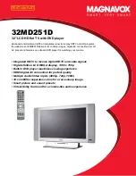
Color TV with Built-In DVD Player
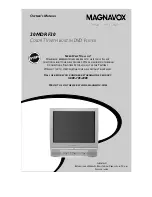
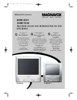
20MC4206/
37
c Copyright 2006 Philips Consumer Electronics B.V. Eindhoven, The Netherlands.
All rights reserved. No part of this publication may be reproduced, stored in a retrieval
system or transmitted, in any form or by any means, electronic, mechanical, photocopying,
or otherwise without the prior permission of Philips.
EN 3139 785 31830
CLASS 1 LASER PRODUCT
KLASSE 1 LASER PRODUKT
KLASS 1 LASER APPARAT
CLASSE 1 PRODUIT LASER
Adjustment Procedures
Schematic Diagrams and CBA's
Exploded Views
Mechanical and Electrical Parts Lists
Service Manual
Service
Service
Service
Contents
Chapter
Survey of versions:
Published by FU-KC 0613 Service AV Systems Printed in The Netherlands Subject to modification
/37 NTSC
Color TV with Built-In DVD Player
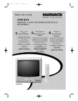
13MC3206/
37
c Copyright 2006 Philips Consumer Electronics B.V. Eindhoven, The Netherlands.
All rights reserved. No part of this publication may be reproduced, stored in a retrieval
system or transmitted, in any form or by any means, electronic, mechanical, photocopying,
or otherwise without the prior permission of Philips.
EN 3139 785 31820
CLASS 1 LASER PRODUCT
KLASSE 1 LASER PRODUKT
KLASS 1 LASER APPARAT
CLASSE 1 PRODUIT LASER
Adjustment Procedures
Schematic Diagrams and CBA's
Exploded Views
Mechanical and Electrical Parts Lists
Service Manual
Service
Service
Service
All manuals and user guides at all-guides.com
all-guides.com
Summary of Contents for 13MC3206/37
Page 12: ...1 4 1 T8201IB OPERATING CONTROLS AND FUNCTIONS All manuals and user guides at all guides com ...
Page 13: ...1 4 2 T8201IB All manuals and user guides at all guides com ...
Page 14: ...1 4 3 T8201IB All manuals and user guides at all guides com ...
Page 15: ...1 4 4 T8201IB All manuals and user guides at all guides com ...