SPECIFICATIONS
Power Source :
220 - 240 V AC 50 Hz
Power Consumption :
10 W
Camera Input :
2:1 interlaced VBS 1.0 V[p-p] / 75
Ω
, 75
Ω
automatic termination / looping through (BNC
connector)
Playback Input :
X1 VBS 1.0V [p-p]/75
Ω
(RCA pin-jack)
Audio Input :
X2 –10 dB/10 k
Ω
(RCA pin-jack)
Monitor Output :
X1 VBS 1.0 V [p-p]/75 (BNC connector)
Recording Output :
X1 VBS 1.0 V[p-p]/75 (RCA pin-jack)
Audio Output :
X2 –10 dB / 100
Ω
(RCA pin-jack)
Audio Monitor Output :
X1 –10 dB / 100
Ω
(RCA pin-jack)
Camera Switching Input :
1 circuit (RCA pin-jack)
Microphone Input :
X4 Switchable –60 dB / 390
Ω
or 0 dB / 390
Ω
Ambient Operating Temperature :
–10 °C - +50 °C
Dimensions :
420 (W) X 44 (H) 350 (D) mm (without projections)
Weight :
3.8
kg
Dimensions and weight are approximate.
Specifications are subject to change without notice.
STANDARD ACCESSORIES
Rack Mount Angle
2 pcs.
Rack Mount Angle Fixing Screw
8 pcs.
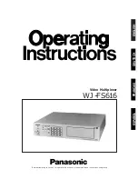
Video Multiplexer
WJ-FS28
ORDER NO. AVS9610196C3
C
1 9 9 6 M a t s u s h i t a C o m m u n i c a t i o n I n d u s t r i a l C o . , L t d .
A l l r i g h t s r e s e r v e d . U n a u t h o r i z e d c o p y i n g a n d
d i s t r i b u t i o n i s a v i o l a t i o n o f l a w .